
Semiconductor device

a semiconductor device and semiconductor technology, applied in semiconductor devices, diodes, electrical equipment, etc., can solve the problems of large surge current flow to circuit elements, difficult to ensure the surge resistance of semiconductor devices, etc., to reduce the size of the second semiconductor device, suppress the surge current, uniformly and stably absorb the surge

Active Publication Date: 2019-03-21
DENSO CORP
View PDF1 Cites 3 Cited by
  • Summary
  • Abstract
  • Description
  • Claims
  • Application Information

AI Technical Summary

Benefits of technology

The patent describes a way to make semiconductor devices that have a smaller size and higher reliability. This is achieved by putting both the cell region and circuit element region on the same semiconductor substrate. This results in better performance and more compact size.

Problems solved by technology

However, there are the following problems when the power-element cells and the circuit elements are arranged on the same semiconductor substrate.
Moreover, due to the above structural features of the elements, an unintentional parasitic structure may be formed between the circuit elements or the power-element cells may electrically interfere with the circuit elements at the boundaries between the power-element cells and the circuit elements.
Therefore, when, for example, a high-speed and high-voltage surge due to an electrostatic discharge is applied, a large amount of surge current may flow to the circuit elements because of the imbalance in impedance between the power-element cells and the circuit elements.
Consequently, when the surge current is locally concentrated to exceed the surge current ratings of the power-element cells or the circuit elements, a latch-up phenomenon may occur, making it difficult to ensure the surge resistance of the semiconductor device.

Method used


Image

  • Semiconductor device
  • Semiconductor device
  • Semiconductor device

Examples


first embodiment

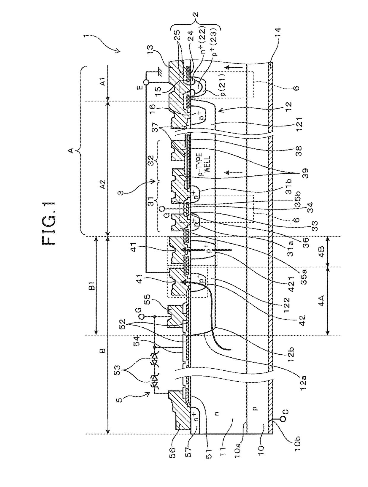
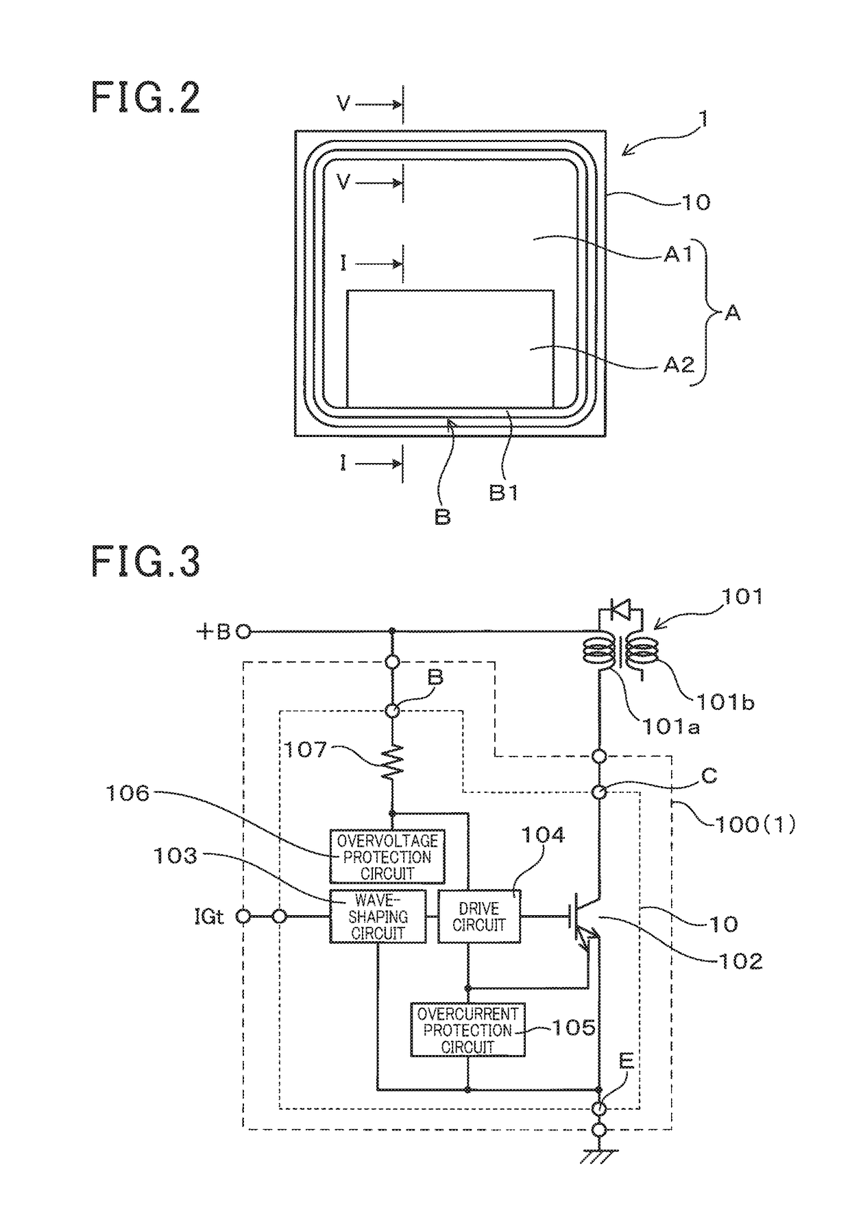
[0034]FIGS. 1 and 2 show the overall configuration of a semiconductor device 1 according to the first embodiment.

[0035]In the present embodiment, the semiconductor device 1 is configured as an intelligent power element in which both a cell region A1 for forming power elements (i.e., power electronic elements) and a circuit element region A2 for forming circuit elements are provided in the same chip.

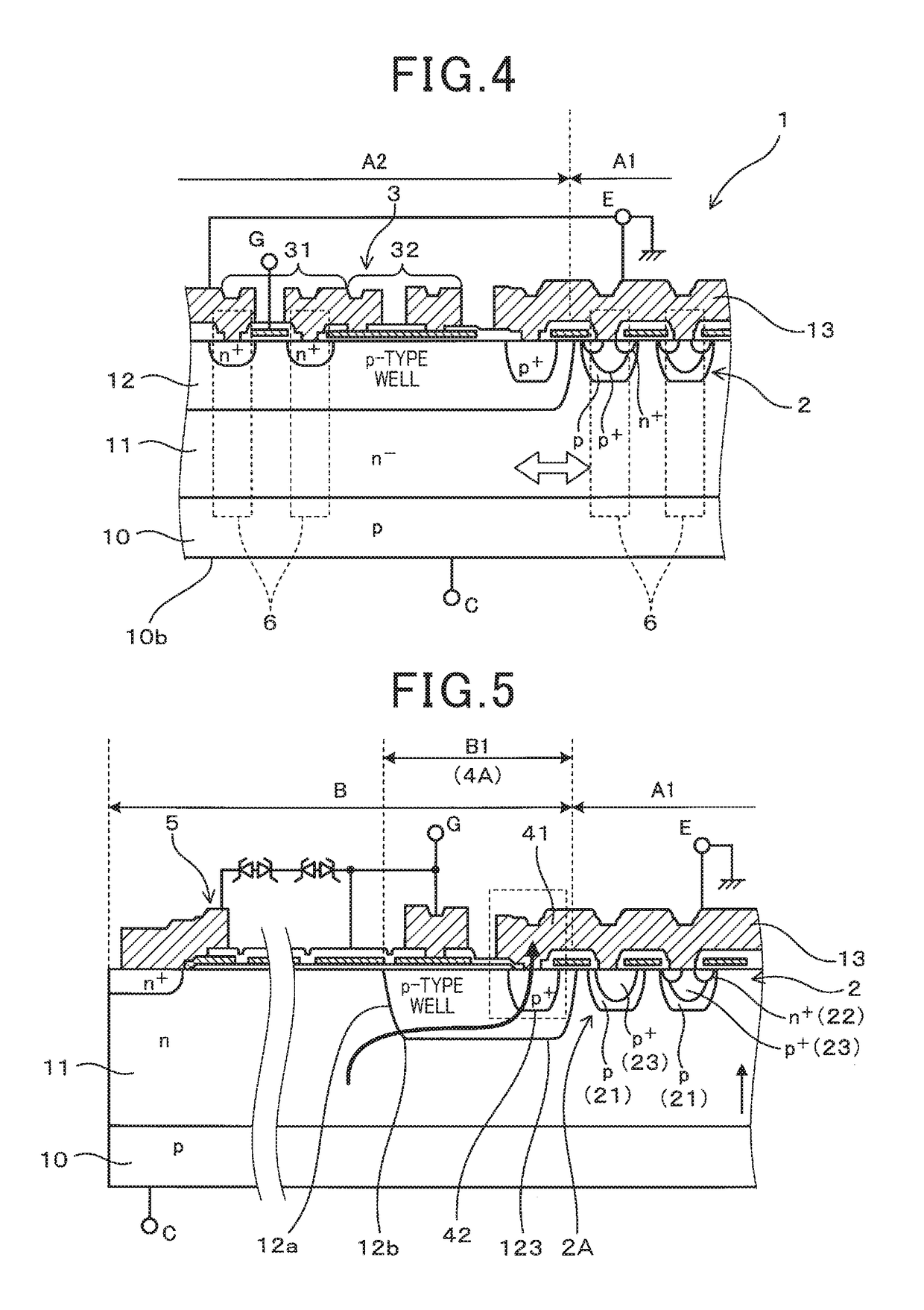
[0036]Moreover, as shown in FIG. 3, the semiconductor device 1 is applied to, for example, an ignition apparatus for an internal combustion engine to constitute an igniter section 100 that controls energization of an ignition coil 101. The igniter section 100 includes a power element 102 (corresponding to the cell region A1) for controlling energization of the ignition coil 101 and circuits (corresponding to the circuit element region A2) for controlling and protecting the power element 102.

[0037]As shown in FIG. 1, the semiconductor device 1 includes a single semiconductor substrate 10 t...

second embodiment

[0112]In the semiconductor device 1 according to the previous embodiment, in the element-forming region A, the shape, size and location of the circuit element region A2 are not particularly limited, but may be suitably modified. Moreover, in the boundary region B1, the number, configuration and location of the voltage-withstanding regions are not particularly limited, but may be suitably modified.

[0113]For example, as shown in FIG. 9, in a semiconductor device 1 according to the second embodiment, the circuit element region A2 is substantially square in shape. The circuit element region A2 is located inside the outer peripheral voltage-withstanding region B, which is substantially square loop-shaped, and close to one of the four curved corner portions of the outer peripheral voltage-withstanding region B. Moreover, the circuit element region A2 adjoins one of the four straight portions of the outer peripheral voltage-withstanding region B over more than half of the entire length of ...

third embodiment

[0124]FIGS. 11 and 12 show the overall configuration of a semiconductor device 1 according to the third embodiment.

[0125]As shown in FIG. 11, in the present embodiment, the element-forming region A is substantially square-shaped and surrounded by the outer peripheral voltage-withstanding region B that is substantially square loop-shaped. The circuit element region A2 is rectangular-shaped and located adjacent to but spaced from one of the four straight portions of the outer peripheral voltage-withstanding region B. More specifically, the circuit element region A2 is spaced at a predetermined interval from the adjacent straight portion of the outer peripheral voltage-withstanding region B. The remaining part of the element-forming region A, where no circuit element region A2 is formed, constitutes the cell region A1. That is, in the present embodiment, the circuit element region A2 is entirely surrounded by the cell region A1. In addition, the cell region A1 and the circuit element r...


PUM


Abstract

A semiconductor device includes a semiconductor substrate having a major surface and both an element-forming region and an outer peripheral voltage-withstanding region that are provided on the major surface side of the semiconductor substrate. The element-forming region includes both a cell region for forming a power element and a circuit element region for forming at least one circuit element. The circuit element region is interposed between the outer peripheral voltage-withstanding region and the cell region. The outer peripheral voltage-withstanding region includes a boundary region that adjoins the element-forming region. In the boundary region, there is provided one or more voltage-withstanding regions. At least one of the one or more voltage-withstanding regions has a withstand voltage lower than both the withstand voltages of the cell region and the circuit element region.

Description

CROSS-REFERENCE TO RELATED APPLICATION[0001]This application is based on and claims priority from Japanese Patent Application No. 2017-179848 filed on Sep. 20, 2017, the contents of which are hereby incorporated by reference in its entirety into this application.BACKGROUND1 Technical Field[0002]The present invention relates to semiconductor devices that include an element-forming region and a voltage-withstanding region.2 Description of Related Art[0003]There are known semiconductor devices which employ power elements (or power electronic elements) such as an IGBT (Insulated Gate Bipolar Transistor) and in which a voltage-withstanding region is provided on the outer peripheral side of a power-element cell region for the purpose of improving the surge resistance.[0004]For example, Japanese Patent No. JP3664129B2 discloses a semiconductor device that has both a first semiconductor region that is of p-type and a voltage-withstanding region provided in a surface region of an n−-type sem...

Claims


Application Information

Patent Timeline
Patent Type & Authority Applications(United States)
IPC IPC(8): H01L29/06H01L29/739H01L29/40H01L29/866
CPCH01L29/0615H01L29/7395H01L29/404H01L29/866H01L29/0603H01L29/0684H01L29/66325H01L29/7393H01L29/861H01L29/16H01L29/78H01L29/405H01L29/0638H01L27/088H01L27/0629H01L21/823493H01L21/823481
Inventor YAMAGUCHI, MOTOO
Owner DENSO CORP
Learn More