

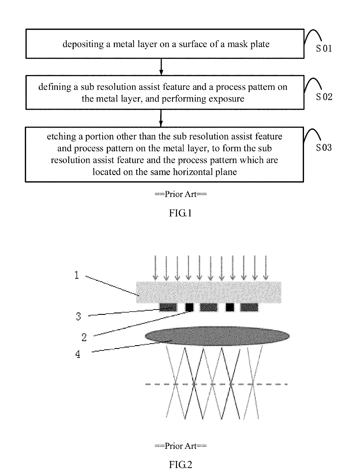
Design method of sub resolution assist feature
- Summary
- Abstract
- Description
- Claims
- Application Information
AI Technical Summary
Benefits of technology
Problems solved by technology
Method used
Image

Examples
Embodiment Construction
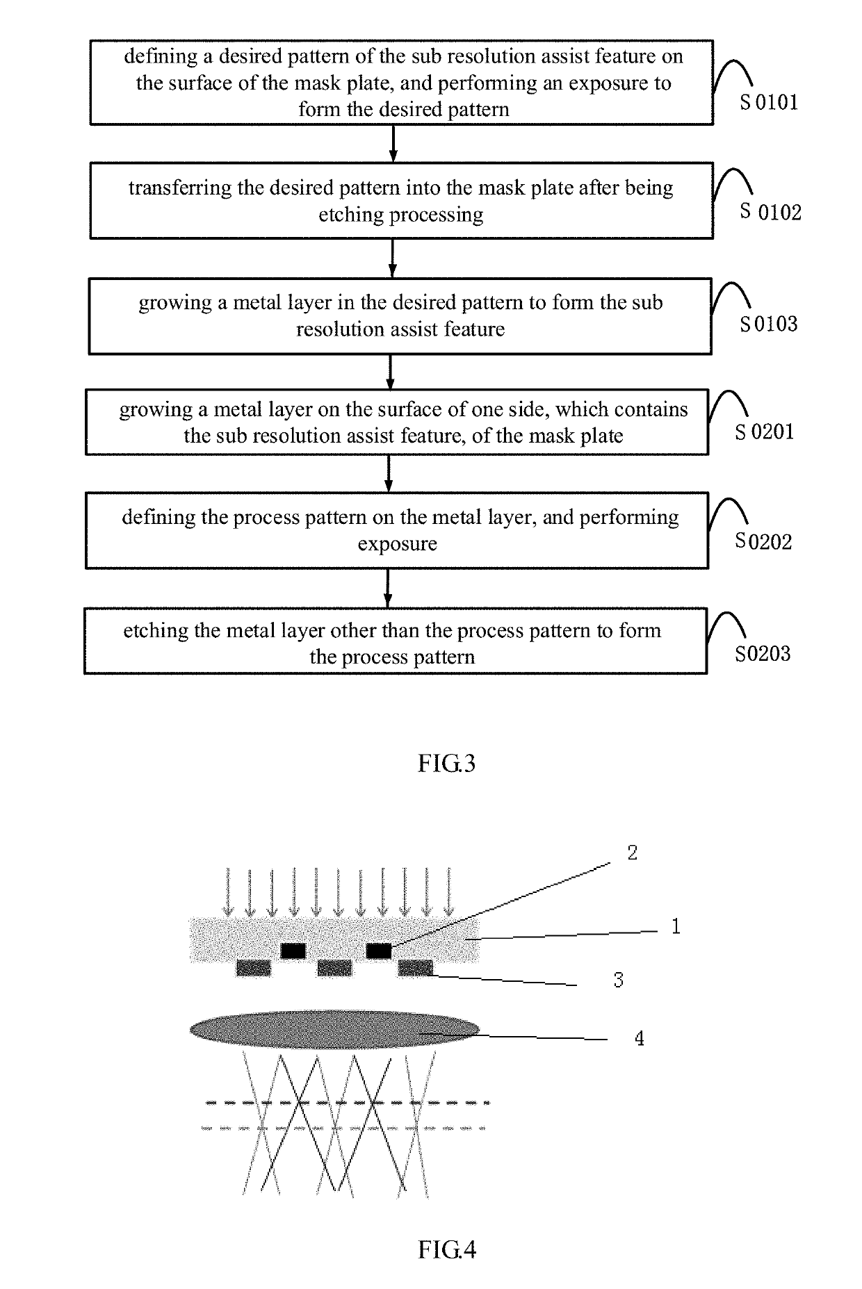
[0043]To make the object, the technical solution and the advantage of the present invention clearer, the specific embodiments of the present invention are described in detail below in combination with drawings.
[0044]As shown in FIG. 3, the present invention provides a design method of a sub resolution assist feature, comprising the following steps of:
[0045]S01: forming a sub resolution assist feature in the mask plate, the upper surface of the sub resolution assist feature is aligned with the upper surface of the mask plate.
[0046]Wherein the thickness of the sub resolution assist feature is less than the thickness of the mask plate, that is to say, in the present invention, the sub resolution assist feature is formed in grooves inside the mask plate, and the upper surface of the grooves are parallel with the upper surface of the mask plate.
[0047]Wherein, the S01 is specifically as follows:
[0048]S0101: defining a desired pattern of the sub resolution assist feature on the surface of ...
PUM
 Abstract
Description
Claims
Application Information