Check patentability & draft patents in minutes with Patsnap Eureka AI!

Semiconductor memory devices, memory systems and methods of operating semiconductor memory devices

Active Publication Date: 2019-05-02
SAMSUNG ELECTRONICS CO LTD
View PDF11 Cites 13 Cited by
  • Summary
  • Abstract
  • Description
  • Claims
  • Application Information

AI Technical Summary

Benefits of technology

The patent describes a semiconductor memory device that can store error bits based on a first command and use them to modify the data being written in the memory cells. The device also has a data input buffer to store the original data and a write data generator to create the modified data. The device can then read and transmit the data back to the memory controller. This technology allows for faster and more efficient memory writing and reading.

Problems solved by technology

However, reducing size may increase bit errors and adversely affect yield.

Method used


Image

  • Semiconductor memory devices, memory systems and methods of operating semiconductor memory devices
  • Semiconductor memory devices, memory systems and methods of operating semiconductor memory devices
  • Semiconductor memory devices, memory systems and methods of operating semiconductor memory devices

Examples


Embodiment Construction

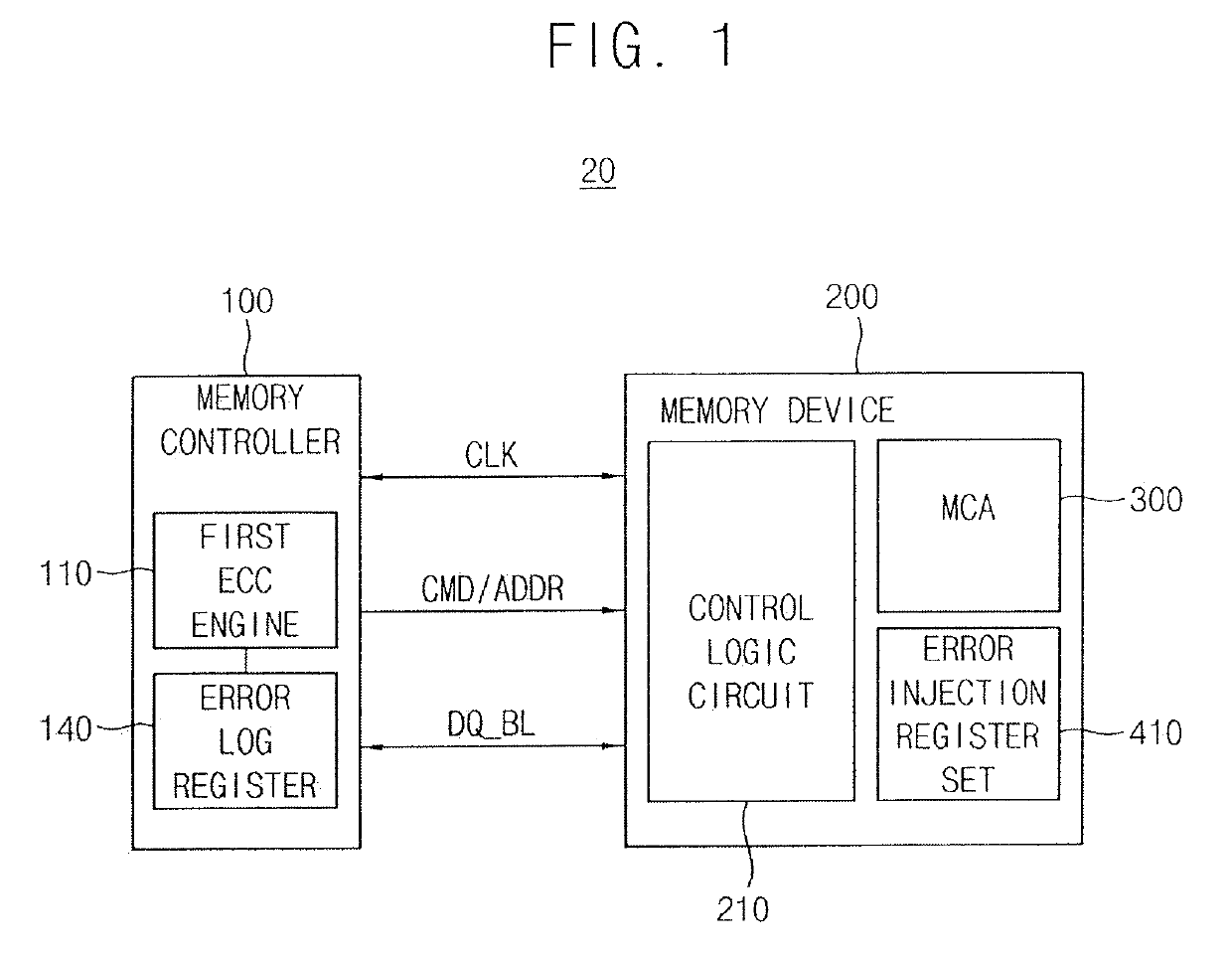
[0024]FIG. 1 illustrates an embodiment of a memory system 20 which may include a memory controller 100 and a semiconductor memory device 200. The memory controller 100 may control overall operation of the memory system 20. The memory controller 100 may control overall data exchange between an external host and the semiconductor memory device 200. For example, the memory controller 100 may write data in the semiconductor memory device 200 and / or read data from the semiconductor memory device 200 based on request from the host. In addition, the memory controller 100 may issue operation commands to the semiconductor memory device 200 for controlling the semiconductor memory device 200.

[0025]The semiconductor memory device 200 may include, for example, dynamic memory cells, and thus may be a dynamic random access memory (DRAM), double data rate 4 (DDR4) synchronous DRAM (SDRAM), or a low power DDR4 (LPDDR4) SDRAM.

[0026]The memory controller 100 transmits a clock signal CLK, a command CM...


PUM


Abstract

A semiconductor memory device which includes a memory cell array, an error injection register set, a data input buffer, a write data generator, and control logic. The error injection register set stores an error bit set, including at least one error bit, based on a first command. The error bit set is associated with a data set to be written in the memory cell array. The data input buffer stores the data set to be written in the memory cell array based on a second command. The write data generator generates a write data set to be written in the memory cell array based on the data set and the error bit set. The control logic controls the error injection register set and the data input buffer.

Description

CROSS-REFERENCE TO RELATED APPLICATION[0001]Korean Patent Application No. 10-2017-0145251, filed on Nov. 2, 2017, and entitled, “Semiconductor Memory Devices, Memory Systems and Methods of Operating Semiconductor Memory Devices,” is incorporated by reference in its entirety.BACKGROUND1. Field[0002]One or more embodiments herein relate to semiconductor memory devices.2. Description of the Related Art[0003]A variety of semiconductor memories have been developed. Non-volatile memories include flash memories. Volatile memories include dynamic random access memories (DRAMs). DRAMs are often used for system memories because of their high speed operation and cost efficiency. Efforts are continually being made to reduce the sizes of these devices. However, reducing size may increase bit errors and adversely affect yield.SUMMARY[0004]In accordance with one or more embodiments, a semiconductor memory device includes a memory cell array; an error injection register set to store an error bit se...

Claims


Application Information

Patent Timeline
IPC IPC(8): G11C29/42G11C29/02G06F11/10G06F11/22
CPCG11C29/42G11C29/02G06F11/1064G06F11/2215G11C29/56004
Inventor SON, JONG-PILSOHN, KYO-MIN
Owner SAMSUNG ELECTRONICS CO LTD
Features
  • R&D
  • Intellectual Property
  • Life Sciences
  • Materials
  • Tech Scout
  • Unparalleled Data Quality
  • Higher Quality Content
  • 60% Fewer Hallucinations
Learn More