Imaging sensor and method for reading out image information

a technology of image information and image sensor, which is applied in the field of image information reading, can solve the problems of ccd sub-array saturating and reaching its full, and achieve the effect of maximizing the signal-to-noise ratio

Active Publication Date: 2019-05-02
INTERUNIVERSITAIR MICRO ELECTRONICS CENT (IMEC VZW)
View PDF7 Cites 6 Cited by
  • Summary
  • Abstract
  • Description
  • Claims
  • Application Information

AI Technical Summary

Benefits of technology

The invention describes a way to combine and read out different filters on the same image sensor using eCCD and imec's monolithic technology. This allows for dynamic selection of image capturing properties and ensures good signal-to-noise ratios for each wavelength band. The number of rows can be different in different CCD sub-arrays, which can be used to optimize the number of active rows and compensate for imager quantum efficiency and / or filter transmission. Overall, the invention allows for more flexible and accurate imaging.

Problems solved by technology

However, there is a risk that the CCD sub-array saturates, i.e. reaches its full well capacity (FWC).

Method used


Image

  • Imaging sensor and method for reading out image information
  • Imaging sensor and method for reading out image information
  • Imaging sensor and method for reading out image information

Examples


Embodiment Construction

[0039]Detailed embodiments of the present invention will now be descried with reference to the drawings.

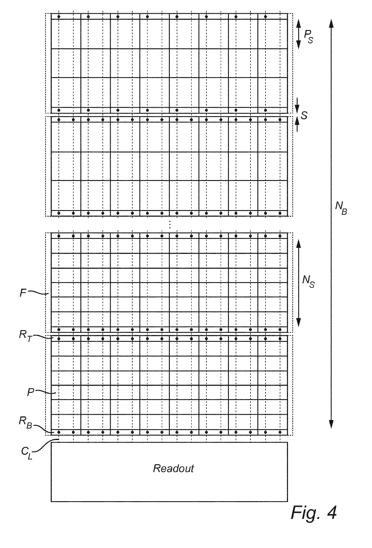
[0040]It is proposed to use multiple CCD TDI arrays on the same chip, which (may or may not) share a single readout. Each CCD sub-array is processed with a dedicated integrated filter (or a combination thereof), which may be a color filter or spectral filter.

[0041]The CCD sub-arrays may be arranged in an embedded CCD (eCCD), as shown in 2014 IEEE International Electron Devices Meeting, 15-17 Dec. 2014, pages: 4.6.1-4.6.4, which combines CMOS with CCD process technology and allows to process CCD gates with CMOS readout and control. The disclosure of how CMOS process technology may be combined with CCD process technology in 2014 IEEE International Electron Devices Meeting, 15-17 Dec. 2014, pages: 4.6.1-4.6.4 is incorporated herein by reference.

[0042]The availability of charge-to-voltage or charge-to-current stages at the output of each CCD sub-array allows to select the wanted CCD s...


PUM


Abstract

An imaging sensor is disclosed, comprising: a set of at least two charge-coupled device, CCD, sub-arrays, wherein each sub-array comprises pixels arranged in columns and rows, and each pixel being arranged to accumulate an electric charge proportional to an intensity of light incident on the pixel; a time delay and integration, TDI, clocking circuitry for controlling and timing transfer of accumulated electric charges between rows of pixels in a column direction in order to integrate the accumulated electric charges in each column of pixels; wherein each CCD sub-array further comprises a readout row for converting the integrated electric charge of each column of pixels into voltage or current, wherein the readout row comprises transistors enabling readout of the signal by the readout block; and a readout block which is arranged to receive input from selected readout rows and convert the input into digital domain or convert the input to a combined representation of pixel values based on the set of CCD sub-arrays.

Description

TECHNICAL FIELD[0001]The present invention relates to an imaging sensor and, in particular, an imaging sensor to be used for time delay integration.BACKGROUND[0002]The combination of Time Delay Integration (TDI) and spectral filtering is useful when the features of TDI are needed (linear movement of a scene, relative to the sensor, and a desire to improve SNR by multiple integration) in combination with an interest in a part of the spectrum by means of filtering. However, traditional CCD TDI image sensors only integrate one CCD TDI array. Hence, a multispectral of color filter combination requires multiple CCD TDI sensors (large, expensive, cumbersome and doesn't scale well), or a filter wheel (cumbersome and filters cannot be used simultaneously). Embedded CCD (eCCD), as shown in 2014 IEEE International Electron Devices Meeting, 15-17 Dec. 2014, pages: 4.6.1-4.6.4, combines CMOS with CCD process technology and allows to process CCD gates with CMOS readout and control.SUMMARY OF THE...

Claims


Application Information

Patent Timeline
IPC IPC(8): H04N5/372H04N5/378H04N5/347
CPCH04N5/37206H04N5/378H04N5/347H04N25/711H04N25/75H04N25/46
Inventor BORREMANS, JONATHANTACK, NICOLAASROSMEULEN, MAARTENGOETSCHALCKX, PAULDE MOOR, PIET
Owner INTERUNIVERSITAIR MICRO ELECTRONICS CENT (IMEC VZW)
Why Eureka
Try Eureka