Light-emitting device and display device using the same

a technology of light-emitting devices and display devices, which is applied in the direction of basic electric elements, semiconductor devices, electrical equipment, etc., can solve the problems of reducing the luminance response speed of the display device, increasing the thickness of the lcd device, and reducing the ability of the display device to be provided with a variety of designs, so as to reduce the defect rate of a transfer process, ensure the effect of electrical connection and minimizing the defect rate of the display devi

Active Publication Date: 2019-05-23
LG DISPLAY CO LTD
View PDF1 Cites 9 Cited by
  • Summary
  • Abstract
  • Description
  • Claims
  • Application Information

AI Technical Summary

Benefits of technology

[0046]Since the n-type electrodes and the p-type electrodes are disposed on the n-type semiconductor layer and the p-type semiconductor layer of the light-emitting device, even in the case in which the light-emitting device is inverted while being disposed on the substrate, electrical connections can be reliably provided. This can accordingly reduce the defect rate of a transfer process used in the fabrication of a display device, thereby minimizing the defect rate of the display device.
[0047]Also provided are a light-emitting device able to reduce damage when abnormal current occurs, and a display device using the same. The light-emitting device may include a p-type semiconductor layer, an active layer, and an n-type semiconductor layer sequentially layered on a substrate. At least one p-type electrode is disposed on the p-type semiconductor layer, while an at least one n-type electrode is disposed on the n-type semiconductor layer. The p-type semiconductor layer includes a first p-type semiconductor layer, a second p-type semiconductor layer, and a first wall by which the first and second p-type semiconductor layers are divided from each other, while the n-type semiconductor layer includes a first n-type semiconductor layer, a second n-type semiconductor layer, and a second wall by which the first and second n-type semiconductor layers are divided from each other. The second n-type semiconductor layer, of the first and second n-type semiconductor layers divided by the first wall, is insulated from the n-type electrode, and at least one first contact hole is provided in the second n-type semiconductor layer to electrically connect the second n-type semiconductor layer to the second p-type semiconductor layer. The second p-type semiconductor layer, of the first and second p-type semiconductor layers divided by the second wall, is insulated from the p-type electrode, and a second contact hole is provided in the second p-type semiconductor layer to electrically connect the second p-type semiconductor layer to the second n-type semiconductor layer. When electrons and holes are supplied to the n-type electrode and the p-type electrode as described above, a forward bias is applied to the first n-type semiconductor layer and the first p-type semiconductor layer while a reverse bias is applied to the second n-type semiconductor layer and the second p-type semiconductor layer.
[0048]As described above, the first and second n-type and p-type semiconductor layers operate regardless of the top portion and the bottom portion of the light-emitting device in order to block current in response to a reverse bias and recombine electrons and holes in response to a forward bias. Accordingly, light-emitting device can provide a light emitting function and a protection function while minimizing damage due to abnormal current.
[0049]According to exemplary embodiments, a light-emitting device may reduce defects caused by the process of disposing the light-emitting device is used. This can consequently reduce defects in a display device that would otherwise occur in the process of displaying light-emitting devices, thereby improving productivity. In addition, the use of the above-described light-emitting device can improve processing convenience.
[0050]According to exemplary embodiments, the use of a light-emitting device able to reduce damage in light-emitting devices and a driving device can improve the reliability of longevity and the reliability of products.

Problems solved by technology

Due to such an additional backlight unit, the thickness of the LCD device may be increased, the ability of the display device to be provided with a variety of designs, such as a flexible structure or a circular profile, may be limited, and the luminance and response speed of the display device may be lowered.
Although organic light-emitting display devices using an organic material are free from separate light sources, they are vulnerable to defective pixels, caused by, for example, oxidation between an organic light-emitting layer and electrodes due to the penetration of moisture and oxygen.
Furthermore, unlike organic light-emitting devices, an LED device is insignificantly influenced by oxygen and moisture, since the LED device uses an inorganic material.
Because of highly expensive semiconductor substrates used to crystallize an inorganic material such as GaN, using a large number of LEDs as light-generating pixels of a display device, rather than using a simple lighting device or a backlight unit, may increase fabrication costs, which is problematic.
In this transfer process, it may be difficult to separate LED devices from the semiconductor substrate.
In addition, there may be significant difficulties in transplanting the separated LED devices properly in intended locations.
The transfer process is related to the productivity of the process of providing a display device, and the method of transferring LED devices one by one is inefficient in terms of mass production.
In the above-described transfer process or a process subsequent to the transfer process, defects may occur in LED devices, i.e., LED devices may be inverted due to process conditions, such as vibrations or heat, while being moved or transferred.
It is significantly difficult to find and repair such defects.
During the separation of the LED devices from the semiconductor substrate by the laser irradiation process, the GaN material of the semiconductor substrate may be subjected to rapid physical expansion due to energy concentration caused by high-energy laser beams, thereby generating impacts.
This may increase defective pixels in a display device, thereby increasing fabrication costs thereof, which is problematic.
However, at this time, due to a sudden flow of current, TFTs, including LED devices, may be damaged.

Method used


Image

  • Light-emitting device and display device using the same
  • Light-emitting device and display device using the same
  • Light-emitting device and display device using the same

Examples


case 3

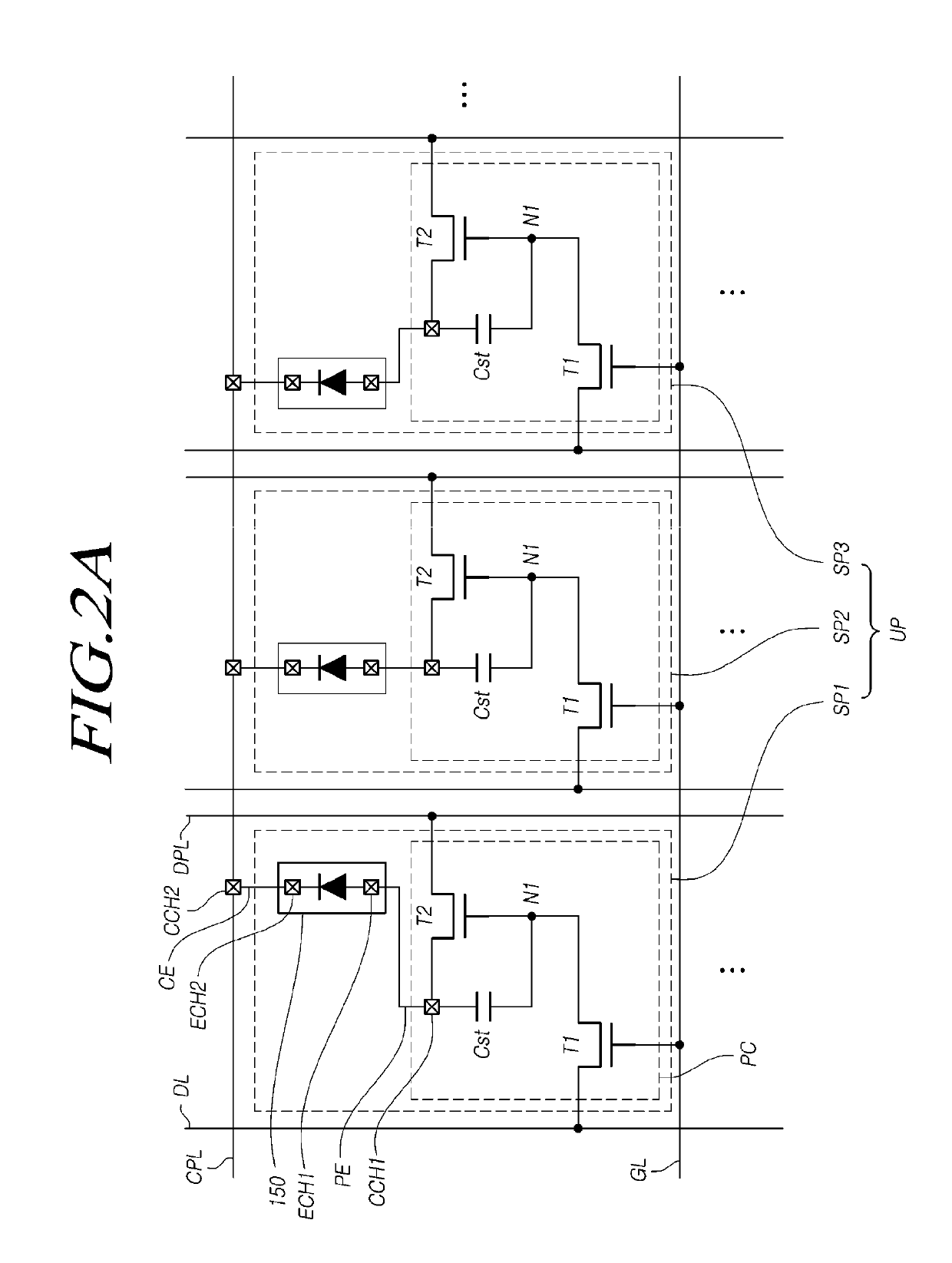
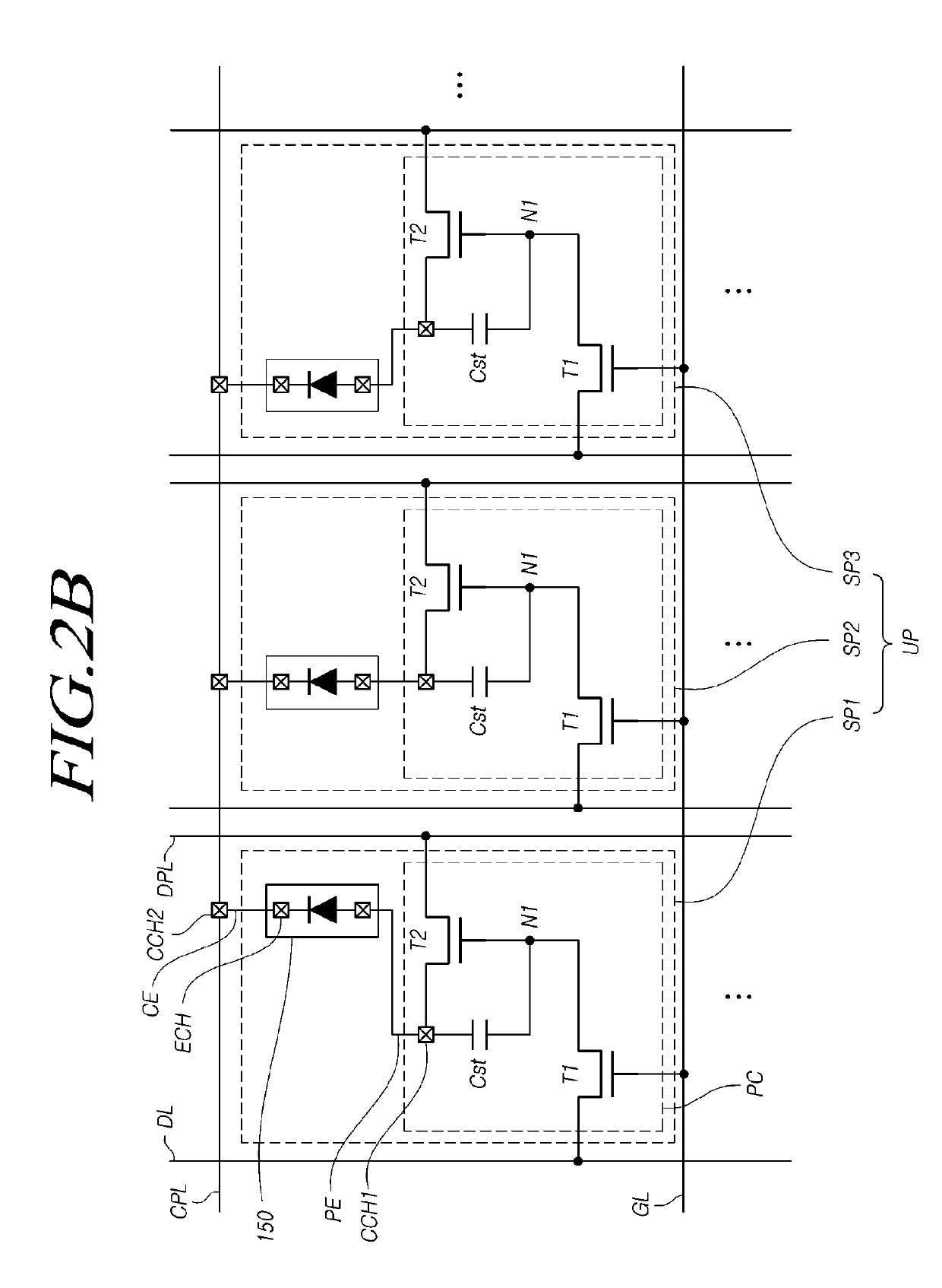
[0247]In Case 3 illustrated in FIG. 11C, the first zone Z1 and the second zone Z2 are set to have independent electrode structures, and one of the first zone Z1 and the second zone Z2 is set as a dummy zone. When the first zone Z1 is damaged or fails to generate light, it is possible to repair a defective pixel by a circuit control method, a laser-based electrode connection method, or the like.

[0248]In addition to the above-described applications, the LED device 150 can be used in a variety of other applications, depending on a variety of circuit connections.

[0249]The connection of electrodes E1 and E2 located on the bottom portions of the LED device 150 may be carried out using a method of melting the butted surfaces of the electrodes using high-temperature heat generated by electrical resistance against current supplied to the adjoined electrodes so that the contact portions of the two electrodes are welded or a method of melting and welding the surfaces of the electrodes connecte...


PUM


Abstract

A light-emitting device and a display device using the same. The light-emitting device improves the reliability of a process of disposing light-emitting devices. The light-emitting device is configured to ensure electrical connections even if the light-emitting device is inverted while being disposed on a substrate. The light-emitting device includes an n-type semiconductor layer and a p-type semiconductor layer. N-type electrodes and p-type electrodes are disposed on both sides of top and bottom surfaces of the light-emitting device. Contact holes are provided to electrically connect one of the n-type electrodes to the n-type semiconductor layer and one of the p-type electrodes to the p-type semiconductor layer. When the light-emitting device is inverted while being disposed on a substrate, the light-emitting device operates ordinarily, thereby reducing the defect rate of a display device.

Description

CROSS REFERENCE TO RELATED APPLICATION[0001]This application claims priority from Korean Patent Application No. 10-2017-0157688, filed on Nov. 23, 2017, and Korean Patent Application No. 10-2017-0167167, filed on Dec. 7, 2017, which are hereby incorporated by reference for all purposes as if fully set forth herein.BACKGROUNDTechnical Field[0002]The present disclosure relates to a light-emitting device and a display device using the same. More particularly, the present disclosure relates to a light-emitting device able to be more firmly disposed in place and a display device using the same.Description of Related Art[0003]Display devices are widely used not only as display screens for TVs or monitors, but also as display screens for notebook computers, tablet computers, smartphones, portable display devices, portable information devices, and the like.[0004]Display devices may be divided into reflective display devices and light-emitting display devices. Reflective display devices disp...

Claims


Application Information

Patent Timeline
Patent Type & Authority Applications(United States)
IPC IPC(8): H01L33/38H01L33/44H01L25/16
CPCH01L33/387H01L33/44H01L25/167H01L33/382H01L33/385H01L33/32H01L33/14H01L33/20H01L2933/0016
Inventor JUNG, TAEILKIM, IL-SOOKWAK, YONGSEOK
Owner LG DISPLAY CO LTD
Why Eureka
Try Eureka