Supercharge Your Innovation With Domain-Expert AI Agents!

SRAM Configuration Cell for Low-Power Field Programmable Gate Arrays

a configuration cell and gate array technology, applied in logic circuits, digital storage, instruments, etc., can solve the problems of static power consumption of fpga, introduce new problems, and long channel devices in the sram cell take up extra die area on the integrated circui

Active Publication Date: 2019-06-06
MICROSEMI SOC
View PDF6 Cites 2 Cited by
  • Summary
  • Abstract
  • Description
  • Claims
  • Application Information

AI Technical Summary

Benefits of technology

The present invention provides a random-access memory cell including complementary bit lines and a word line, which is controlled by a programming potential and an operating potential during programming and read modes of operation. The cell includes pairs of series-connected cross-coupled p-channel and n-channel hybrid FinFET transistors connected between the voltage supply nodes, which allow for faster data processing and reduced power consumption during programming and read modes of operation. The integrated circuit includes multiple memory cells with the same configuration, further optimizing data processing speed and reducing power consumption.

Problems solved by technology

There are a few drawbacks to the use of the memory cell of FIG. 1.
An undersirable consequence of using a transistor having a low Vt is that the n-channel switch transistor will leak current from its source to drain terminals even when its gate is at ground and the device is shut off This unnecessarily contributes to the static power consumption of the FPGA.
This arrangement disclosed in Telikepalli addresses the three issues mentioned above, but introduces new problems.
First, the long channel devices in the SRAM cell takes up extra die area on the integrated circuit.
In addition, the need to provide a device having an additional medium-thickness oxide for the SRAM cell complicates the manufacturing process.
As technology has advanced to feature sizes below 40 nm, and transistor geometry has evolved from planar geometry to FinFET geometry, it is no longer feasible to provide such non-standard medium thickness oxide devices.
Below 20 nm, when process technology changes from planar to FinFET transistors, it becomes even more difficult to continue to support a special non-standard medium-thickness oxide.
However, because a pair of devices instead of a single device is used, the area of the switch is increased, and the leakage is not improved.
Furthermore, the need to bring both the true (Y) and complement (Y!) outputs of the SRAM cell to the switch devices requires a significant increase in layout area due to additional metal layer wiring requirements.

Method used


Image

  • SRAM Configuration Cell for Low-Power Field Programmable Gate Arrays
  • SRAM Configuration Cell for Low-Power Field Programmable Gate Arrays
  • SRAM Configuration Cell for Low-Power Field Programmable Gate Arrays

Examples


Embodiment Construction

[0024]Persons of ordinary skill in the art will realize that the following description of the present invention is illustrative only and not in any way limiting. Other embodiments of the invention will readily suggest themselves to such skilled persons.

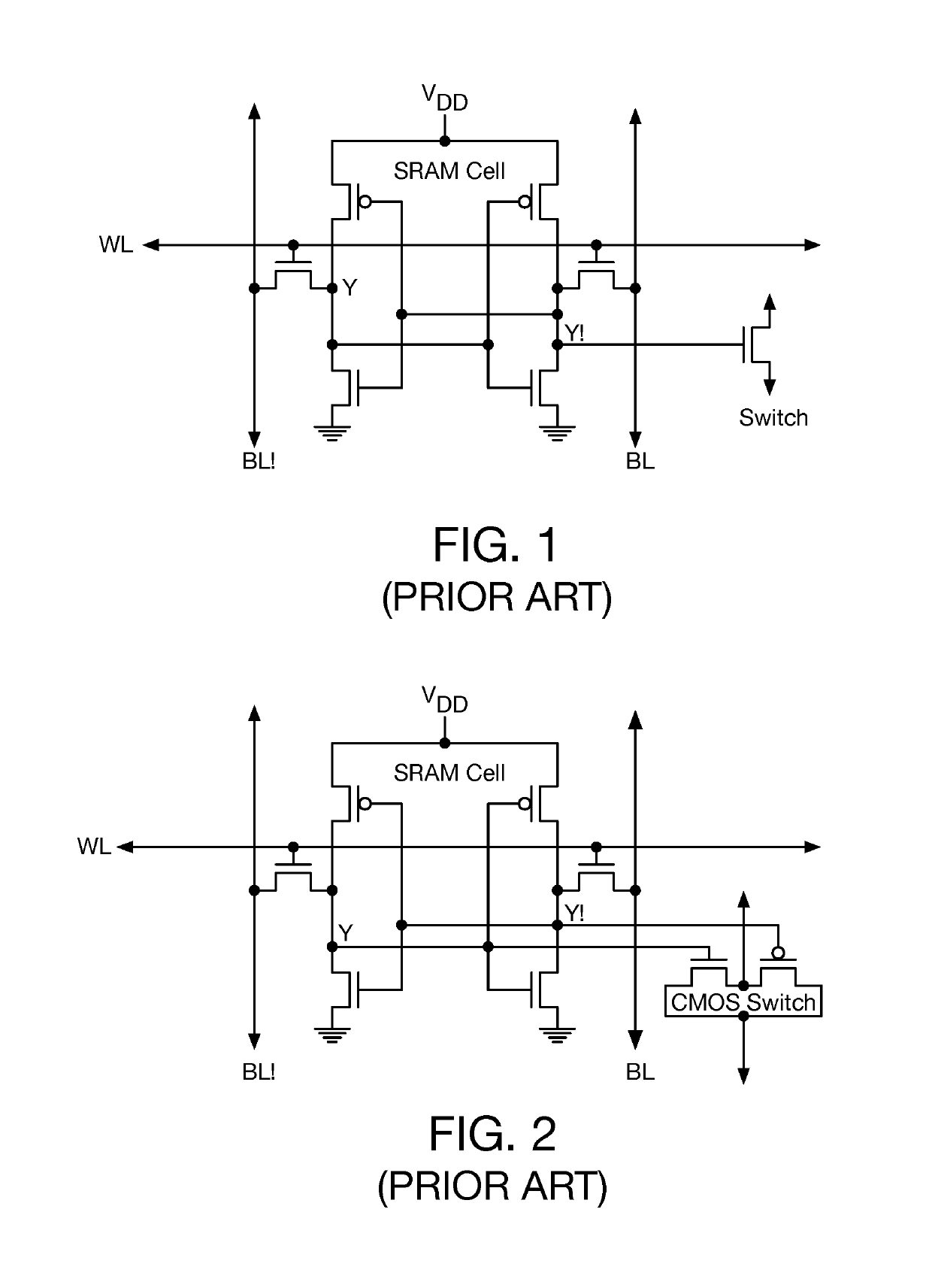
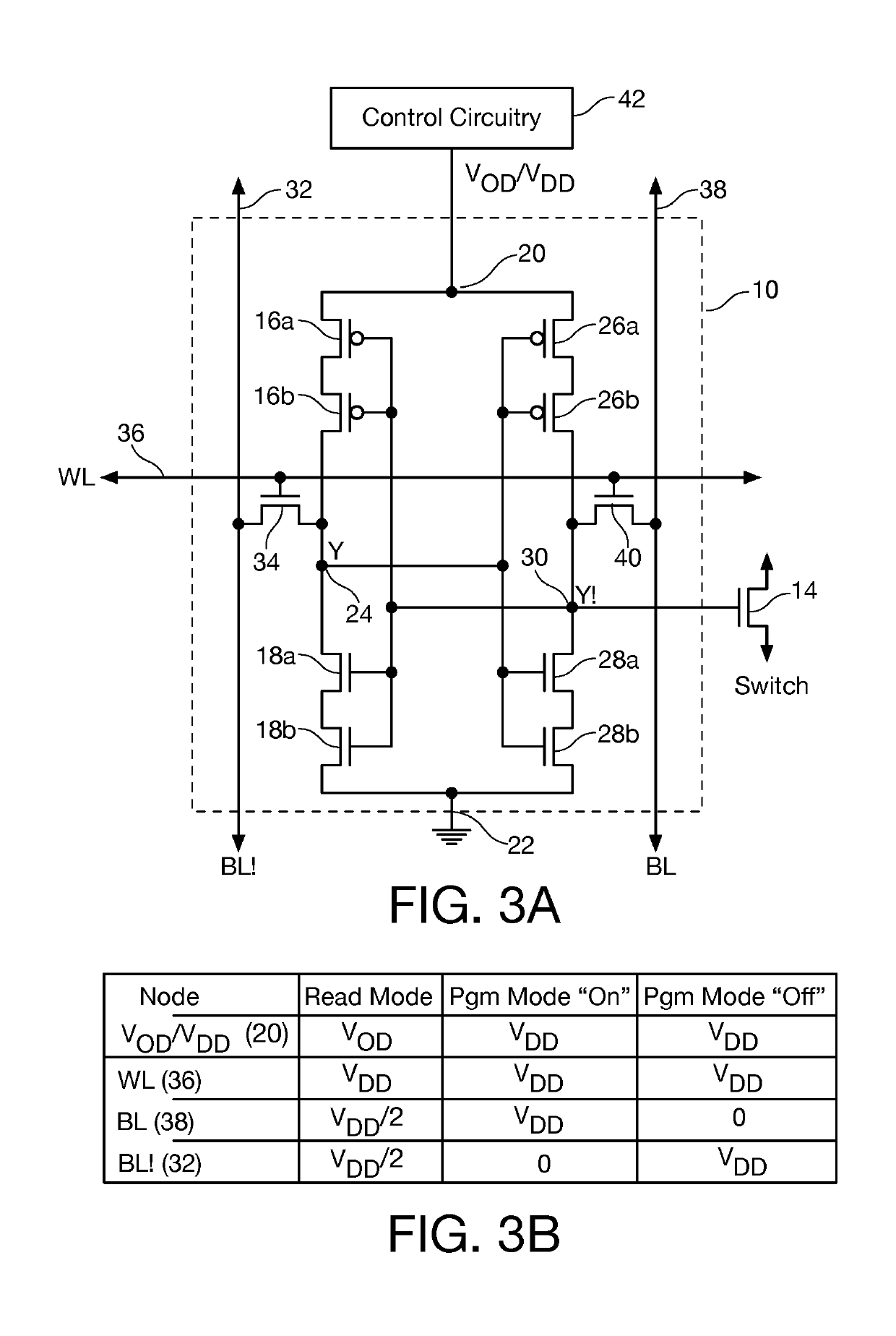
[0025]Referring now to FIG. 3A, a 10-transistor static random-access memory (SRAM) configuration cell (shown within dashed region 10) driving the gate of an n-channel transistor switch 14 for use in a user-programmable integrated circuit such as an FPGA is shown. It is to be understand that a configuration cell does not require high speed switching, since the cell is set at initial configuration, and is generally not changed thereafter. The SRAM configuration cell 10 includes a first pair of series-connected p -channel FinFET transistors 16a and 16b in series with a first pair of series-connected re- channel FinFET transistors 18a and 18b disposed between two voltage supply rails 20 and 22. The drains of the second of the first pair o...


PUM


Abstract

A random-access memory cell includes first and second voltage supply nodes, first and second complementary output nodes, first and second complementary bit lines associated with the memory cell, and a word line associated with the memory cell. Pairs of series-connected cross-coupled p-channel and n-channel hybrid FinFET transistors are connected between the voltage supply nodes, the first bit line coupled to the first output node, and the second bit line coupled to the second output node.

Description

BACKGROUND[0001]The present invention relates to user-programmable integrated circuits such as field programmable gate array integrated circuits. More particularly, the present invention relates to static random-access memory configuration cells for use in user-programmable integrated circuit devices such as field programmable gate array (FPGA) integrated circuits.[0002]FIG. 1 shows a prior-art 6-transistor static random-access memory (SRAM) cell driving the gate of an n-channel switch transistor for use in a user-programmable integrated circuit such as an FPGA. The SRAM cell includes a first p-channel transistor in series with a first n-channel transistor between VDD and ground. The gates of the first p-channel transistor and the first n-channel transistor are connected together. The drains of the first p-channel transistor and the first n-channel transistor are connected together to define a first output node Y.[0003]A second p-channel transistor is connected in series with a seco...

Claims


Application Information

Patent Timeline
Patent Type & Authority Applications(United States)
IPC IPC(8): G11C11/412G11C11/419H03K19/177
CPCG11C11/412G11C11/419H03K19/1776
Inventor GREENE, JONATHAN W.MCCOLLUM, JOHN
Owner MICROSEMI SOC
Features
  • R&D
  • Intellectual Property
  • Life Sciences
  • Materials
  • Tech Scout
  • Unparalleled Data Quality
  • Higher Quality Content
  • 60% Fewer Hallucinations
Learn More