Multilayer ceramic electronic component

Pending Publication Date: 2019-06-13
MURATA MFG CO LTD
View PDF17 Cites 3 Cited by
  • Summary
  • Abstract
  • Description
  • Claims
  • Application Information

AI Technical Summary

Benefits of technology

[0008]Preferred embodiments of the present invention provide multilayer ceramic electronic components that are each capable of achieving compatibilit

Problems solved by technology

However, there is a limit to the high withstand voltage design within a range of the standard dimensions of the multilayer ceramic capacitor.
This is because when the number of divided internal electrodes is increased to increase the number of the opposing portions of the i

Method used


Image

  • Multilayer ceramic electronic component
  • Multilayer ceramic electronic component
  • Multilayer ceramic electronic component

Examples


first preferred embodiment

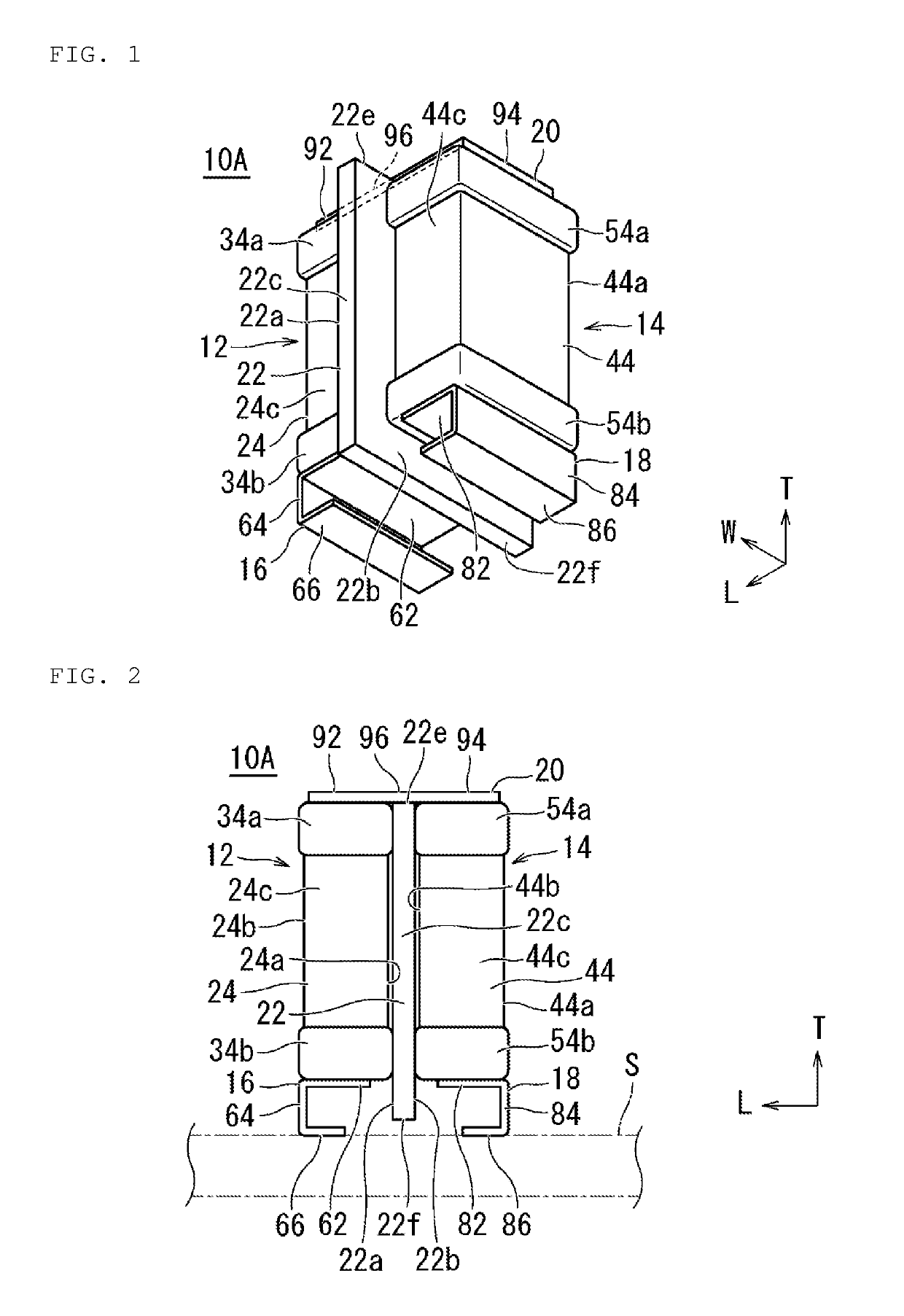
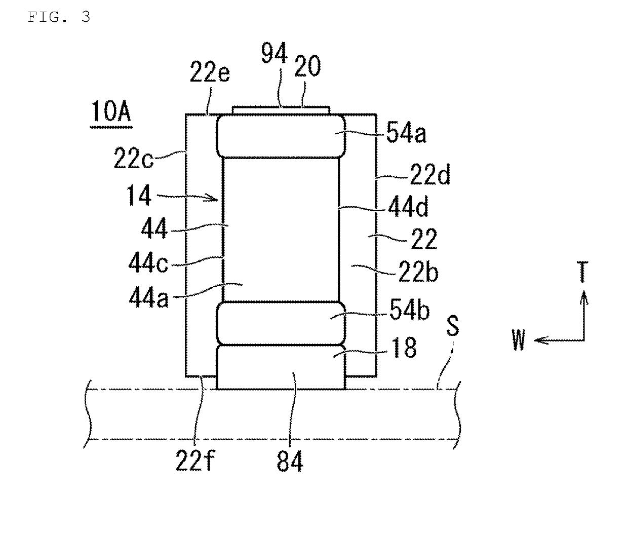
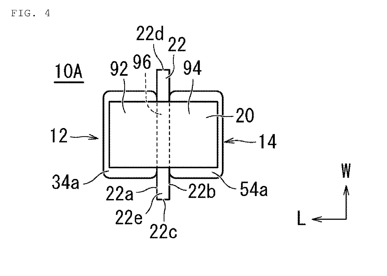
[0059]A multilayer ceramic electronic component according to a first preferred embodiment of the present invention will be described. FIG. 1 is an external perspective view illustrating the multilayer ceramic electronic component of the first preferred embodiment of the present invention. FIG. 2 is a front view of the multilayer ceramic electronic component in FIG. 1. FIG. 3 is a side view of the multilayer ceramic electronic component in FIG. 1. FIG. 4 is a plan view of the multilayer ceramic electronic component in FIG. 1.

[0060]As illustrated in FIGS. 1 to 4, a multilayer ceramic electronic component 10A includes a first multilayer ceramic electronic component body 12, a second multilayer ceramic electronic component body 14, a first metal terminal 16, a second metal terminal 18, a connection terminal 20, and an insulator 22. In FIGS. 1 to 4, a symbol T indicates a height direction of the multilayer ceramic electronic component 10A, a symbol L indicates a length direction of the m...

second preferred embodiment

[0264]A multilayer ceramic electronic component according to a second preferred embodiment of the present invention will be described. FIG. 26 is a front view illustrating the multilayer ceramic electronic component of the second preferred embodiment of the present invention. A multilayer ceramic electronic component 10B of the second preferred embodiment is similar to the multilayer ceramic electronic component 10A of the first preferred embodiment in FIG. 1 except for the insulator. Thus, the same or similar portions as those of the multilayer ceramic electronic component 10A are denoted by the same reference numerals, and the description thereof is omitted.

[0265]As illustrated in FIG. 26, an insulator 400 (denoted by a two-dot chain line) is preferably a resin, for example, and the resin is disposed between the first multilayer ceramic electronic component body 12 and the second multilayer ceramic electronic component body 14, and disposed so as to cover the first multilayer cera...

third preferred embodiment

[0274]A multilayer ceramic electronic component according to a third preferred embodiment of the present invention will be described. FIG. 30 is a front view illustrating the multilayer ceramic electronic component of the third preferred embodiment of the present invention. A multilayer ceramic electronic component 10C of the third preferred embodiment is similar to the multilayer ceramic electronic component 10B of the second preferred embodiment in FIG. 26 except for the metal terminal and the connection terminals. Therefore, the same or similar portions as those of the multilayer ceramic electronic component 10B are denoted by the same reference numerals, and the description thereof is omitted.

[0275]As illustrated in FIG. 30, a first metal terminal 316 is connected to the first external electrode 34a of the first multilayer ceramic electronic component body 12 using a bonding material. The second metal terminal 318 is connected to the third external electrode 54a of the second mu...


PUM

PropertyMeasurementUnit
Thicknessaaaaaaaaaa
Thicknessaaaaaaaaaa
Thicknessaaaaaaaaaa

Abstract

A multilayer ceramic electronic component includes an end surface of a second external electrode and an end surface of a fourth external electrode that face a mounting surface of a mounting substrate on which a first multilayer ceramic electronic component body and a second multilayer ceramic electronic component body are mounted. A first metal terminal is connected to the second external electrode, a second metal terminal is connected to the fourth external electrode, and a connection terminal is connected across a first external electrode and a third external electrode. An insulator is disposed between the first multilayer ceramic electronic component body and the second multilayer ceramic electronic component body.

Description

CROSS REFERENCE TO RELATED APPLICATIONS[0001]This application claims the benefit of priority to Japanese Patent Application No. 2017-236342 filed on Dec. 8, 2017. The entire contents of this application are hereby incorporated herein by reference.BACKGROUND OF THE INVENTION1. Field of the Invention[0002]The present invention relates to a multilayer ceramic electronic component, and particularly, to a multilayer ceramic electronic component suitable for a high withstand voltage.2. Description of the Related Art[0003]In recent years, miniaturization and high capacitance of a multilayer ceramic capacitor is advancing due to miniaturization and surface mounting of an electronic device. Such a trend also spreads to medium and high voltage capacitors for a backlight and a switching power supply of a liquid crystal display. Thus, in the field of high-withstand voltage multilayer ceramic capacitor, there is also a demand for a smaller and high-capacitance multilayer ceramic capacitor.[0004]...

Claims


Application Information

Patent Timeline
IPC IPC(8): H01G4/38H01G4/232H01G4/248H01G4/012H01L41/083H01L41/047H01L41/053
CPCH01G4/38H01G4/232H01G4/248H01G4/012H01L41/083H01L41/0471H01L41/0472H01L41/0475H01L41/053H01G4/30H01G4/1227H01G4/1236H01L41/1876H10N30/872H10N30/871H10N30/875H10N30/88H10N30/50H10N30/8536H10N30/8554
Inventor TOGAWA, MAKOTO
Owner MURATA MFG CO LTD
Why Eureka
Try Eureka