Signal trace fan-out method for double-sided mounting on printed circuit board and printed circuit board

Inactive Publication Date: 2019-07-04
CELESTICA TECH CONSULTANCY SHANGHAI
View PDF27 Cites 2 Cited by
  • Summary
  • Abstract
  • Description
  • Claims
  • Application Information

AI Technical Summary

Benefits of technology

The present invention relates to a method for mounting components on both sides of a printed circuit board (PCB). The method involves providing blind vias on the top and bottom layers of the PCB and fanning out signal traces of components on either surface through the blind vias. This allows for successful signal traces fan-out when connectors are mounted at the same positions on both layers of the PCB and ensures good signal integrality. The technical effects of the invention are improved signal quality and reliable connections between components on both sides of a PCB.

Problems solved by technology

However, such design requirement brings difficulties and challenges to fan-out of signal traces of the high-density QSFP-DD connector on the PCB, and integrality at 56 Gbps.

Method used


Image

  • Signal trace fan-out method for double-sided mounting on printed circuit board and printed circuit board
  • Signal trace fan-out method for double-sided mounting on printed circuit board and printed circuit board
  • Signal trace fan-out method for double-sided mounting on printed circuit board and printed circuit board

Examples


Embodiment Construction

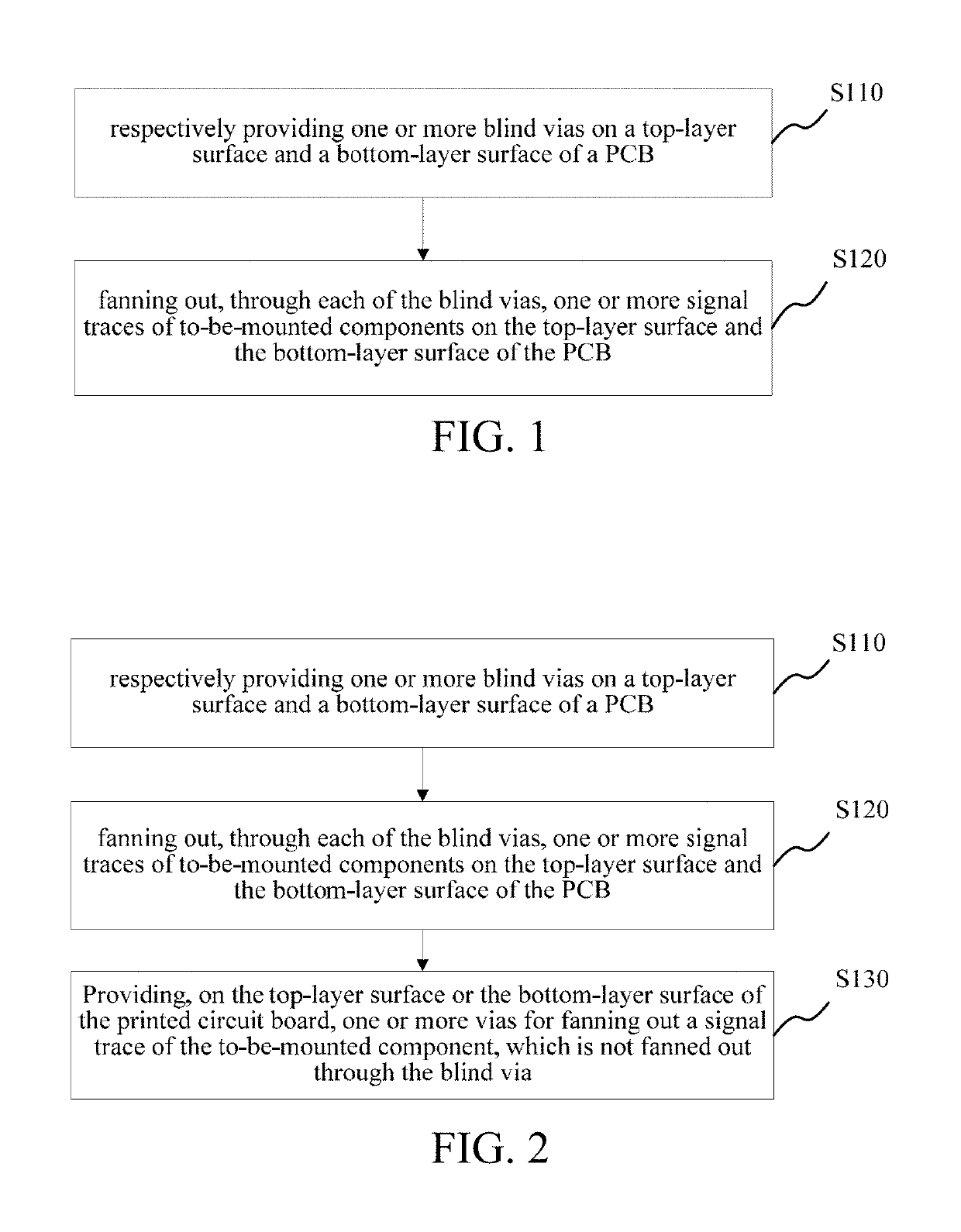
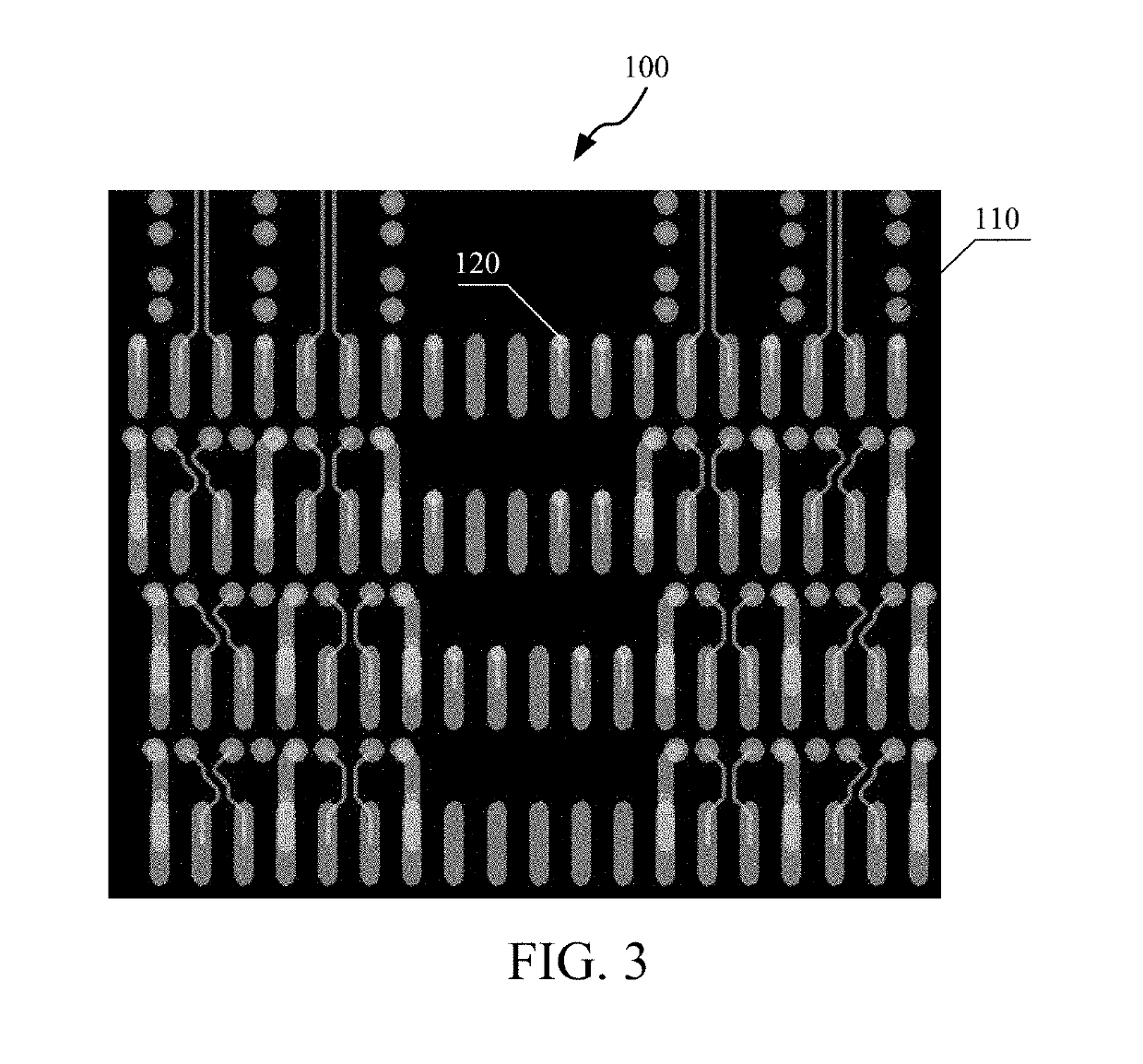
[0021]The embodiments of the present invention will be described through specific embodiments in the following. One skilled in the art can easily understand other advantages and effects of the present invention according to contents disclosed by the description. The present invention can also be implemented or applied through other different specific embodiments. Various modifications or changes can also be made to all details in the description based on different points of view and applications without departing from the spirit of the present invention. It needs to be stated that the following embodiments and the features in the embodiments can be combined with one another under the situation of no conflict.

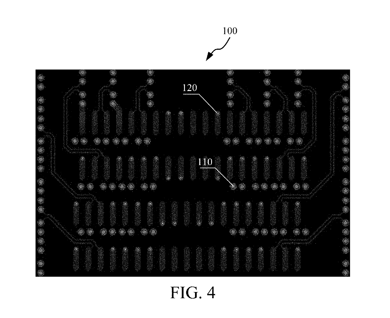
[0022]Referring to FIG. 1 to FIG. 4, it should be noted that structures, scales, and sizes illustrated in the accompanying drawings of this specification in cooperation with the contents disclosed in this specification are all used for those skilled in the art understanding and ...


PUM


Abstract

The present invention provides a signal trace fan-out method for double-sided mounting on a PCB, including: respectively providing one or more blind vias on the top-layer surface and the bottom-layer surface of a PCB; and fanning out, through each of the blind vias, one or more signal traces of to-be-mounted components on the top-layer surface and the bottom-layer surface of the PCB. The number and positions of the blind vias are set based on the size of routing space when the to-be-mounted component is mounted on the top-layer surface or the bottom-layer surface of the PCB. In a manner of combining the blind vias with through holes, the present invention achieves successful fan-out of the signal traces when QSFP-DD connectors are mounted at same positions on both the top layer and the bottom layer of the PCB, and ensures relatively good signal integrality.

Description

BACKGROUND OF THE PRESENT INVENTIONField of Invention[0001]The present invention relates to the field of electronic circuits, in particular to the technical field of mounting, and specifically to a signal trace fan-out method for double-sided mounting on a printed circuit board (PCB) and a PCB.DESCRIPTION OF RELATED ARTS[0002]In the next-generation 400G network switch product, a high-density QSFP-DD connector is used as I / O port. QSFP means Quad Small Form-Factor Pluggable. A transmission rate of a Quad Small Form-Factor Pluggable reaches 40 Gbps. Both the speed and the density of the four-channel pluggable interface are better than those of a four-channel CX4 interface. A small pluggable QSFP connector can satisfy multiple supply protocols of MSA, and can greatly simplify design work of users, including signal integrality of a host connector, squirrel-cage EMI shielding of a module, heat dissipation and a light pipe signal solution. The length of passive and active copper trace ass...

Claims


Application Information

Patent Timeline
IPC IPC(8): H05K1/11H05K1/18H05K3/46H05K3/42H05K3/40
CPCH05K1/116H05K1/181H05K3/4623H05K3/421H05K3/4038H05K2201/10189H05K1/0216H05K2201/093H05K1/113H05K2201/09227H05K2201/09509
Inventor WEN, JIWEIFENG, CHENXIACHEN, LIANGQU, LIJUAN
Owner CELESTICA TECH CONSULTANCY SHANGHAI
Why Eureka
Try Eureka