
Semiconductor device

a technology of semiconductors and devices, applied in logic circuit coupling/interface arrangements, digital storage, instruments, etc., can solve problems such as load capacitance, delay in output signals, and deterioration of image quality

Active Publication Date: 2019-07-18
LAPIS SEMICON CO LTD
View PDF7 Cites 22 Cited by
  • Summary
  • Abstract
  • Description
  • Claims
  • Application Information

AI Technical Summary

Benefits of technology

The solution enables high-speed amplification operations that effectively follow input signal level changes, improving display quality by reducing delays and display unevenness, thereby enhancing the performance of semiconductor devices in driving increased load capacitances.

Problems solved by technology

Accordingly, an increase in the load capacitances of the data lines and a reduction in the driving period may prevent the amplification operation from following a level change of the input video signal, and cause a delay in the output signals.
This may cause deterioration in image quality, such as display unevenness.
This impairs a significant increase in the amplification speed, thus causing deterioration in display quality.

Method used


Image

  • Semiconductor device
  • Semiconductor device
  • Semiconductor device

Examples


first embodiment

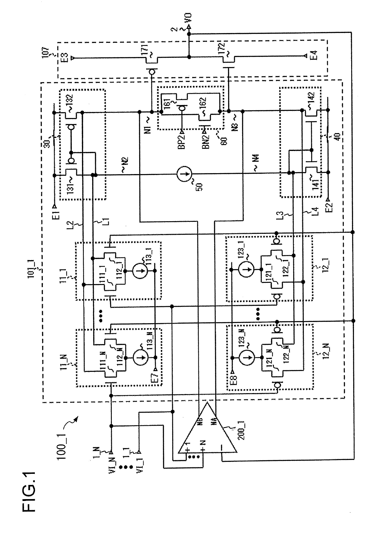
[0039]FIG. 1 is a circuit diagram of a first embodiment of an output circuit, as a semiconductor device according to the present invention. In the following description, a P-channel MOS (metal oxide semiconductor) transistor is referred to as a Pch transistor, and an N-channel MOS transistor is referred to as an Nch transistor.

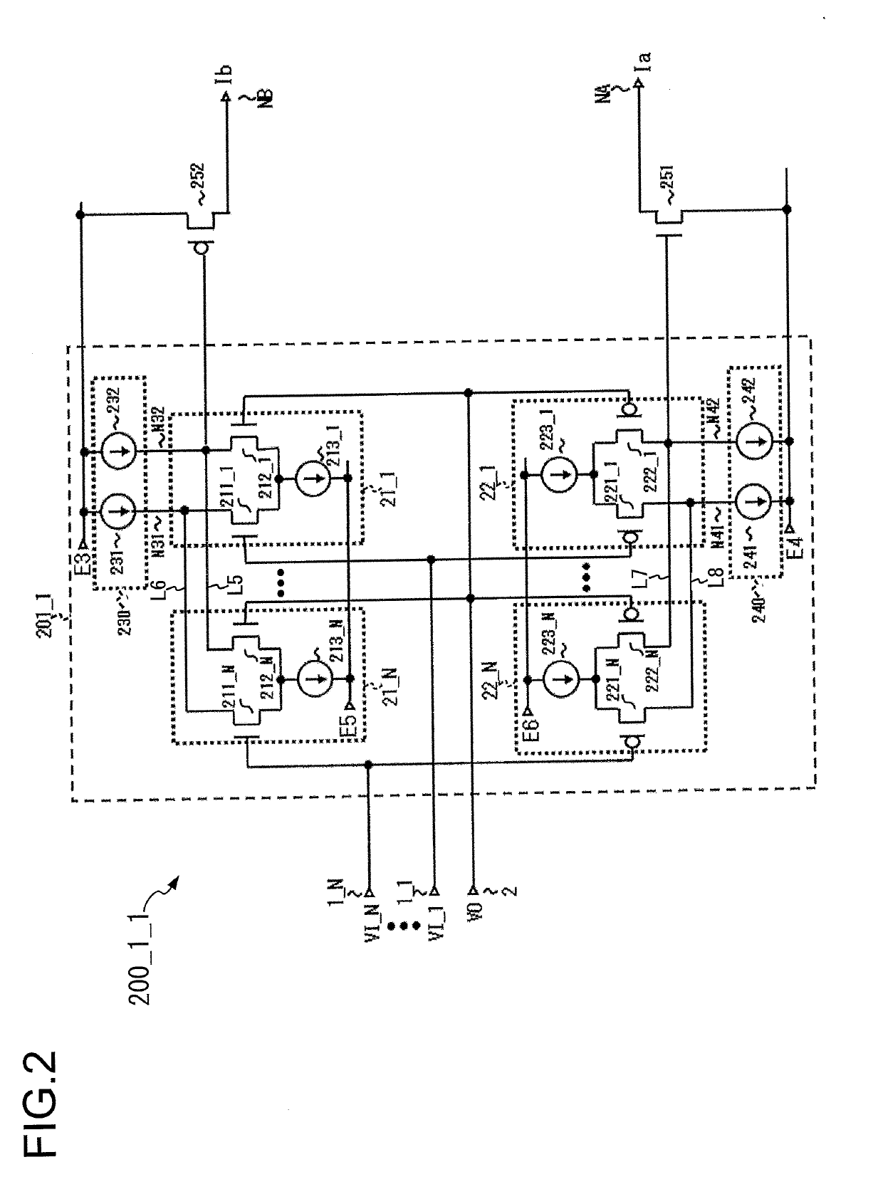
[0040]As illustrated in FIG. 1, an output circuit 100_1 includes a differential input stage 101_1, an output amplifier stage 107, and an amplification accelerator circuit 200_1.

[0041]The differential input stage 101_1 generates a P-channel drive potential and an N-channel drive potential on the basis of the potential difference between each of input signal voltages VI_1 to VI_N to be inputted to first to Nth (N is an integer of 1 or more) input terminals 1_1 to 1_N, respectively, and an output signal voltage VO of an output terminal 2. The differential input stage 101_1 supplies the P-channel drive potential to a gate of the Pch transistor 171 of the output am...

second embodiment

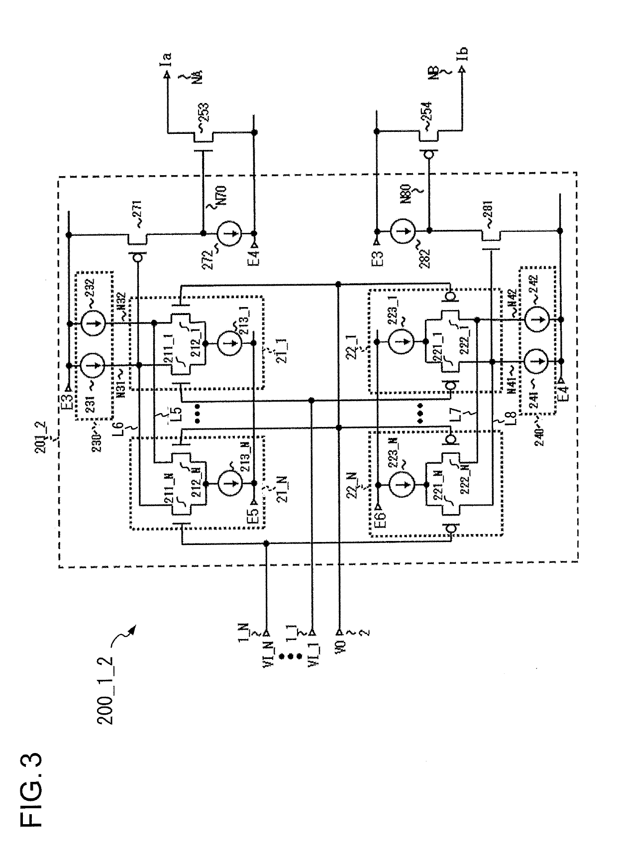
[0151]FIG. 5 is a circuit diagram of an output circuit 100_2 according to a second embodiment of the output circuit as the semiconductor device according to the present invention. Note that the output circuit 100_2 illustrated in FIG. 5 adopts an amplification accelerator circuit 200_2 instead of the amplification accelerator circuit 200_1 illustrated in FIG. 1. The other configuration of the output circuit 100_2 is the same as that of FIG. 1. Thus, the description of the same configuration as that of FIG. 1 is omitted.

[0152]The amplification accelerator circuit 200_2 includes four output nodes NA, NB, NC, and ND, as first to fourth output nodes. The amplification accelerator circuit 200_2 first performs a comparison between the weighted average voltage of the first to Nth input signal voltages VI_1 to VI_N and the output signal voltage VO.

[0153]At this time, when the output signal voltage VO is higher than the weighted average voltage of the first to Nth input signal voltages VI_1 ...

third embodiment

[0166]FIG. 7 is a circuit diagram of an output circuit 100_3 according to a third embodiment of the output circuit as the semiconductor device according to the present invention. Note that the output circuit 100_3 illustrated in FIG. 7 adopts a differential input stage 101_2 instead of the differential input stage 101_1 illustrated in FIG. 1. The other configuration of the output circuit 100_3 is the same as that of FIG. 1. At this time, in the differential input stage 101_2 illustrated in FIG. 7, low voltage cascode current mirrors 30A and 40A are substituted for the current mirrors 30 and 40 of FIG. 1. The configuration of the current mirrors 30A and 40A will next be described. The other configuration is the same as that of the output circuit 100_1 of FIG. 1, so a description thereof is omitted.

[0167]The Pch current mirror 30A is constituted of a low voltage cascode current mirror connected between the first power supply terminal E1 and the node pair (N1 and N2). Specifically, the...


PUM


Abstract

A current corresponding to the difference between an input signal voltage and an output signal voltage is generated as an amplification acceleration current. The amplification acceleration current is sent to an output node of a current mirror, which drives a transistor in an output amplifier stage, and therefore added to a current to drive the transistor in the output amplifier stage.

Description

CROSS-REFERENCE TO THE RELATED APPLICATIONS[0001]This is a continuation of U.S. application Ser. No. 15 / 442,107, filed on Feb. 24, 2017, and allowed on Nov. 26, 2018, which claims the benefit of priority from Japanese Patent Application 2016-35475 filed on Feb. 26, 2016. The entire disclosures of these prior U.S. and foreign applications are incorporated herein by reference.BACKGROUND OF THE INVENTION1. Field of the Invention[0002]The present invention relates to a semiconductor device, and more specifically, to a semiconductor device including output circuits that output voltage signals for driving loads.2. Description of the Related Art[0003]Currently, active-matrix liquid crystal displays, organic EL displays, and the like have spread into the mainstream of display devices. Such a display device is equipped with a display panel having a matrix of display cells connected to a plurality of data lines, and a data driver for driving the data lines of the display panel.[0004]Due to in...

Claims


Application Information

Patent Timeline
Patent Type & Authority Applications(United States)
IPC IPC(8): G09G3/20G11C19/00H03K19/0175G09G3/36
CPCG09G3/2092G11C19/00H03K19/017509G09G3/3696G09G2330/028G09G2310/0291G09G2310/08G09G2310/0286G09G2310/0289
Inventor TSUCHI, HIROSHINISHIMIZU, MANABUSYUTOU, YUUSHI
Owner LAPIS SEMICON CO LTD
Learn More