Active matrix substrate and method for producing same

a technology of active matrix substrate and substrate, which is applied in the direction of identification means, instruments, semiconductor devices, etc., can solve the problems of difficult reduction (frame-narrowing) of frame area, known technology, etc., and achieve the effect of pixel aperture ratio and light transmittance of active matrix substra

Active Publication Date: 2019-08-01
SHARP KK
View PDF0 Cites 6 Cited by
  • Summary
  • Abstract
  • Description
  • Claims
  • Application Information

AI Technical Summary

Benefits of technology

[0030]According to the embodiments, it is possible that a pixel aperture ratio and the light transmittance of an active matrix substrate in which a drive circuit that includes an oxide semiconductor TFT is provided within a pixel are increased.

Problems solved by technology

On the other hand, technologies are known that monolithically (integrally) provide a drive circuit, such as a gate driver or a source driver, in a frame area.
In the configuration described above, when a surface size of a display device in which the active matrix substrate finds application is increased, in some cases, a circuit scale of the gate driver 910 is also increased, and a reduction (frame-narrowing) of a frame area is difficult to achieve.

Method used


Image

  • Active matrix substrate and method for producing same
  • Active matrix substrate and method for producing same
  • Active matrix substrate and method for producing same

Examples


first embodiment

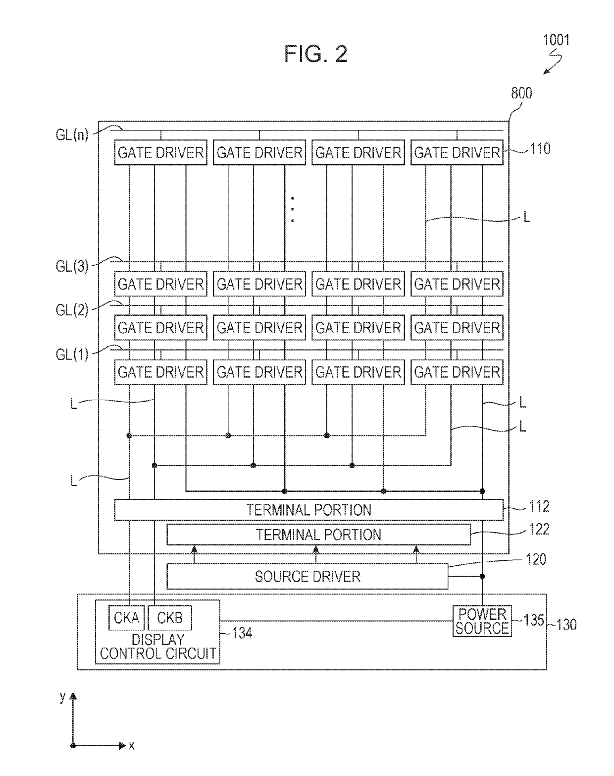
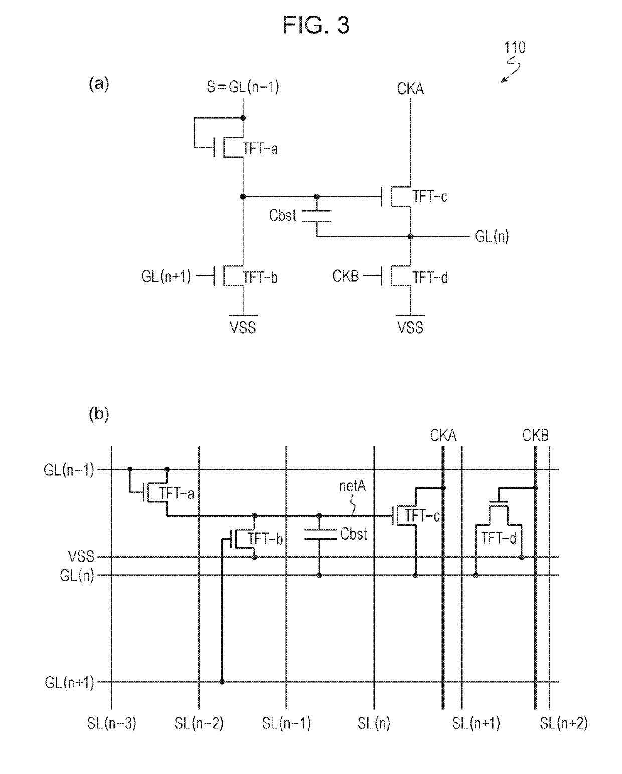
[0044]An active matrix substrate according to a first embodiment of the present invention will be described below with reference to the drawings. The active matrix substrate according to the present embodiment has a monolithic gate driver within a display area. The source driver, for example, is provided in the active matrix substrate, using a COG mounting method.

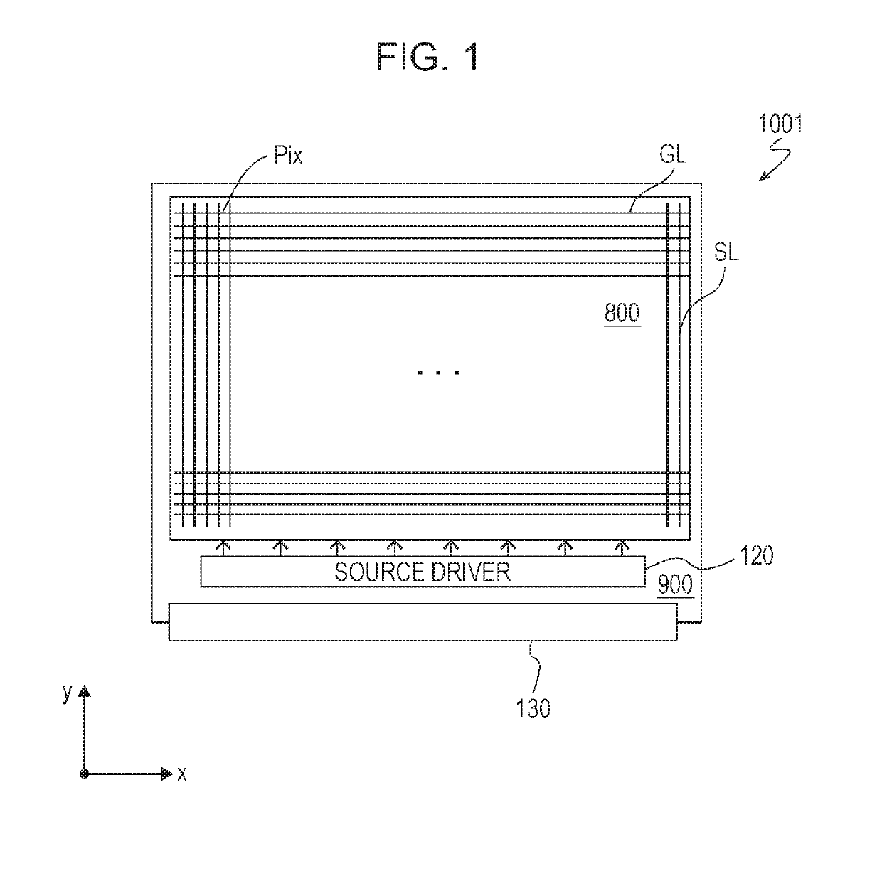
[0045]FIG. 1 is a plan-view diagram illustrating an outline of an active matrix substrate 1001 according to the present embodiment.

[0046]As illustrated in FIG. 1, the active matrix substrate 1001 includes multiple pixel areas Pix that are arranged in matrix form in a first direction x and a second direction y, multiple gate bus lines GL that extend in the first direction x, and multiple source bus lines SL that extend in the second direction y. An area 800 that includes the multiple pixel areas Pix, of the active matrix substrate 1001 is referred to as “display area”, and an area 900 that is positioned in the vicinity of th...

second embodiment

[0112]An active matrix substrate according to a second embodiment of the present invention will be described below with reference to the drawings. The semiconductor device according to the present embodiment is an active matrix substrate that includes an oxide semiconductor TFT and a crystalline silicon TFT that are formed on the same substrate.

[0113]The active matrix substrate according to the present embodiment includes the first circuit TFT that constitutes a pixel TFT and a drive circuit (for example, a gate driver), in the display area, and includes a second circuit TFT in the non-display area. The second circuit TFT is a circuit TFT that constitutes a peripheral circuit that is monolithically formed in the non-display area. This peripheral circuit may be a Source Shared Driving (SSD) circuit, an inspection circuit, a drive circuit (for example, a source driver), or the like.

[0114]The pixel TFT and the first circuit TFT are oxide semiconductor TFTs that are the same as describe...

third embodiment

[0135]An active matrix substrate according to a third embodiment of the present invention will be described below with reference to the drawings. The semiconductor device according to the present embodiment is an active matrix substrate that includes an oxide semiconductor TFT and a crystalline silicon TFT that are formed on the same substrate.

[0136]A difference from the active matrix substrate 1003 according to the second embodiment is that in the present embodiment, at least a portion of the drive circuit wiring line L is formed using a crystalline silicon film that is the same as the crystalline silicon semiconductor layer 31. Specifically, the drive circuit wiring line L according to the present embodiment includes first and second metal portions that are formed from a gate metal film or a source metal film, and a connection portion that is formed from a crystalline silicon film and that electrically connects the first metal portion and the second metal portion.

[0137]FIG. 10 is ...


PUM

PropertyMeasurementUnit
thicknessaaaaaaaaaa
thicknessaaaaaaaaaa
thicknessaaaaaaaaaa

Abstract

An active matrix substrate (1001) has multiple pixel areas. At least one pixel area includes a pixel TFT (20), a pixel electrode (15), a first circuit TFT (10), and drive circuit wiring lines (L1 to L3) that are connected to the first circuit TFT. The pixel TFT (20) and the first circuit TFT (10) are oxide semiconductor TFTs. The pixel electrode (15) is formed from an upper transparent conductive film. The drive circuit wiring line includes a transparent wiring line portion (L1 and L2) that is formed from a lower transparent conductive film which is positioned closer to a substrate 1 than the upper transparent conductive film. At least one of a source electrode (8) and a drain electrode (9) of the first circuit TFT (10) is formed from the lower transparent conductive film.

Description

TECHNICAL FIELD[0001]The present invention relates to an active matrix substrate and a method for manufacturing the active matrix substrate.BACKGROUND ART[0002]An active matrix substrate that is used in a liquid crystal display device or the like includes a switching element, such as a Thin Film Transistor (hereinafter referred to as “TFT”), for every pixel. As this switching element, a TFT of which an active layer is an amorphous silicon film (hereinafter referred to as “amorphous silicon TFT”), or a TFT of which an active layer is a polycrystalline silicon film (hereinafter referred to as “polycrystalline silicon TFT”) has been widely used in the related art. In the present specification, the TFT that is positioned as the switching element for every pixel is referred to as “pixel TFT”. Furthermore, a portion that corresponds to a pixel of a display device, of the active matrix substrate is referred to as “pixel” or “pixel area”.[0003]It has been proposed that instead of amorphous ...

Claims


Application Information

Patent Timeline
Patent Type & Authority Applications(United States)
IPC IPC(8): H01L27/12G02F1/1362G02F1/1368
CPCH01L27/1225H01L27/1248H01L27/127G02F1/1368G02F1/136286G02F1/136277G09F9/00G09F9/30H01L27/1251H01L29/7869G02F1/13454G02F2201/40G09G3/20G09G2300/0426G09G2310/0286G09G2310/0267G09G3/3674G09G3/3688G02F1/13685G02F1/1343G02F1/133H01L29/4908H10K59/123H10K59/131H10K59/1213
Inventor MATSUKIZONO, HIROSHI
Owner SHARP KK
Why Eureka
Try Eureka