
Imaging device

a technology of imaging device and irradiation control, which is applied in the direction of irradiation control device, television system, transistor, etc., can solve problems such as image deterioration, and achieve the effect of reducing noise and reducing leakage curren

Active Publication Date: 2019-08-01
PANASONIC INTELLECTUAL PROPERTY MANAGEMENT CO LTD
View PDF6 Cites 5 Cited by
  • Summary
  • Abstract
  • Description
  • Claims
  • Application Information

AI Technical Summary

Benefits of technology

The patent text is about a method to reduce noise in imaging devices. It suggests that reducing dark current, which is electric current that can affect the quality of the image, can help to improve image quality. The patent describes an imaging device that can suppress dark current, resulting in better quality images.

Problems solved by technology

In an imaging device, a resultant image might deteriorate due to leak current from or to an impurity region that accumulates charges generated through photoelectric conversion.

Method used


Image

  • Imaging device
  • Imaging device
  • Imaging device

Examples


first embodiment

Modification of First Embodiment

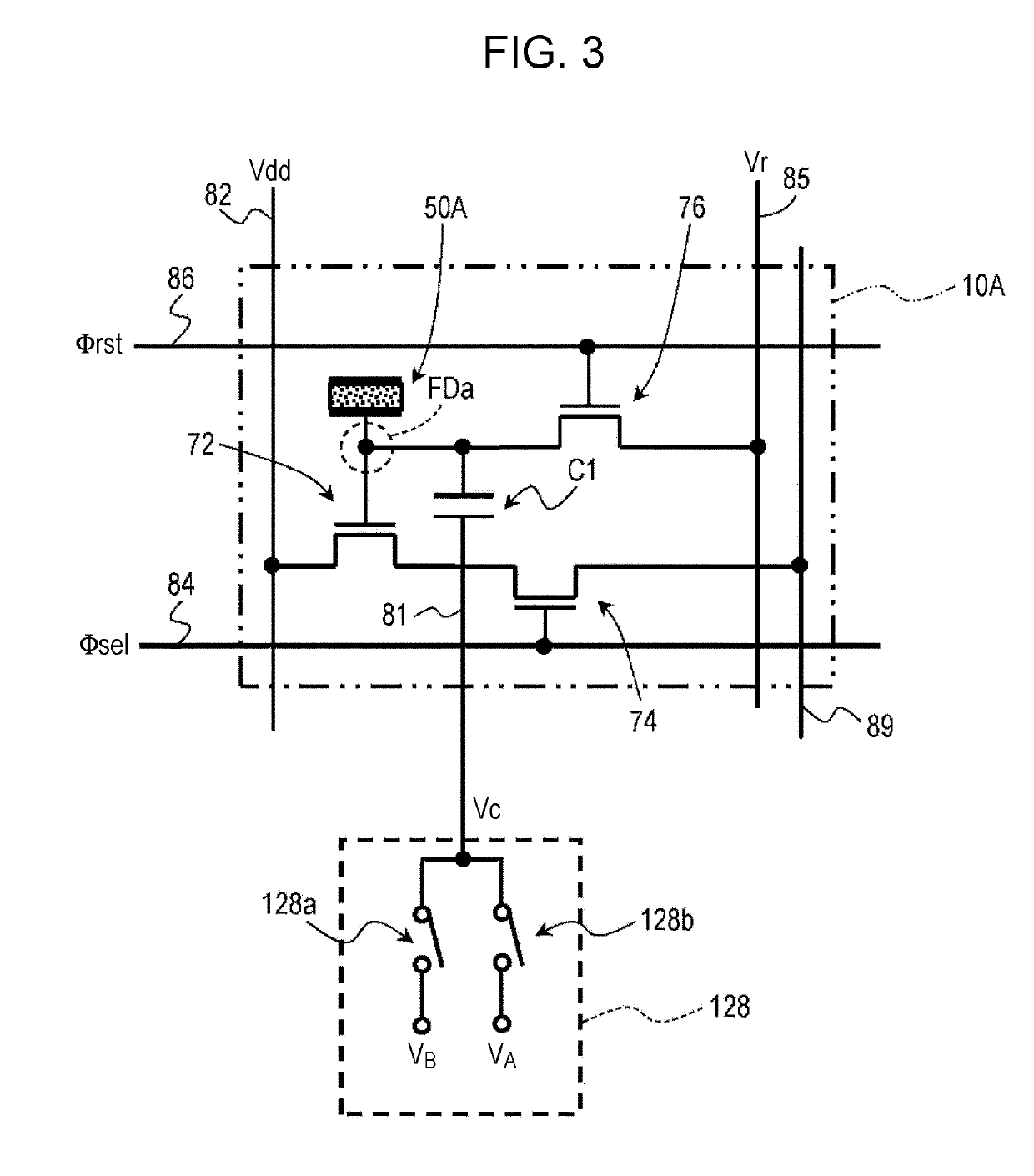
[0234]The imaging device 100 in the present disclosure is not limited to a multilayer imaging device. FIG. 5 schematically illustrates another example of the circuit configuration of the pixel 10. Unlike the pixel 10A described with reference to FIG. 3, a pixel 10Ap illustrated in FIG. 5 includes a photoelectric conversion unit 50B instead of the photoelectric conversion unit 50A. The photoelectric conversion unit 50B is, for example, an embedded photodiode formed in the semiconductor substrate 60.

[0235]As illustrated in FIG. 5, the photoelectric conversion unit 50B is connected to the gate of the signal detection transistor 72 in this example. In the configuration illustrated in FIG. 5, a node FDb between the photoelectric conversion unit 50B and the signal detection transistor 72 corresponds to a charge accumulation node. In other words, a p-n junction in the embedded photodiode, which is the photoelectric conversion unit 50B, the impurity region 60...

second embodiment

Modifications of Second Embodiment

[0298]FIG. 15 illustrates an imaging device according to a modification of the second embodiment of the present disclosure. In the circuit configuration of a pixel 10Bp illustrated in FIG. 15, the photoelectric conversion unit 50A of the pixel 10B illustrated in FIG. 12 is replaced by the photoelectric conversion unit 50B.

[0299]The operation of the imaging device 100 including the pixel 10Bp may be the same, for example, as that described with reference to FIG. 14A or 14B. That is, in the first period, in which the reset transistor 76 is on, the first voltage VA may be applied to the impurity region 60b, and in the second period, which comes after the reset transistor 76 is turned off and in which the transistor 78 is off, the second voltage VB may be applied to the impurity region 60b.

[0300]With the circuit configuration illustrated in FIG. 15, as with that of the pixel 10B illustrated in FIG. 12, the potential of the node RD, which is a floating ...

third embodiment

[0322]FIGS. 19A and 19B schematically illustrate examples of the circuit configuration of a pixel included in an imaging device according to a third embodiment of the present disclosure. An imaging device 140 illustrated in FIG. 19A includes a pixel 10D. As with the circuit configuration described with reference to FIG. 3, the pixel 10D includes the signal detection transistor 72, the address transistor 74, and the reset transistor 76. In the circuit configuration of a pixel 10Dp illustrated in FIG. 19B, the photoelectric conversion unit 50A of the pixel 10D illustrated in FIG. 19A is replaced by the photoelectric conversion unit 50B.

[0323]A main difference between the pixel 10D illustrated in FIG. 19A and the pixel 10A described with reference to FIG. 3 is that, in the pixel 10D, the voltage supply circuit 128 is not connected to the node FDa and the node FDa and the address signal line 84 are electrically connected to each other through the capacitor C1. The pixel 10D has the devi...


PUM


Abstract

An imaging device includes a semiconductor substrate that includes a first impurity region having n-type conductivity; a photoelectric converter that is electrically connected to the first impurity region and that converts light into charges; a capacitor that includes a first terminal and a second terminal, the first terminal being electrically connected to the first impurity region; and a voltage supply circuit electrically connected to the second terminal. The voltage supply circuit is configured to generate a first voltage and a second voltage different from the first voltage. The first impurity region accumulates positive charges generated by the photoelectric converter.

Description

BACKGROUND1. Technical Field[0001]The present disclosure relates to an imaging device.2. Description of the Related Art[0002]Charge-coupled device (CCD) image sensors and complementary metal-oxide-semiconductor (CMOS) image sensors are widely used in digital still cameras, digital cameras, and the like. As generally known, such an image sensor includes photodiodes formed on a semiconductor substrate.[0003]A structure has also been proposed in which a photoelectric conversion unit including a photoelectric conversion layer is provided above a semiconductor substrate (e.g., refer to International Publication No. 2012 / 147302). An imaging device having such a structure is called a “multilayer imaging device”. A multilayer imaging device includes a floating node that is electrically connected to a photoelectric conversion unit and that temporarily accumulates, as signal charges, positive or negative charges generated through photoelectric conversion. The floating node typically includes ...

Claims


Application Information

Patent Timeline
IPC IPC(8): H04N5/361H01L27/146H04N5/369
CPCH04N5/361H01L27/14643H01L27/14612H04N5/369H01L27/14636H01L27/14634H01L27/14665H04N25/59H04N25/76H04N25/63H04N25/68H04N25/62H01L27/146H04N25/70
Inventor SATOU, YOSHIAKIYAMADA, SHOTAMURAKAMI, MASASHIHIROSE, YUTAKA
Owner PANASONIC INTELLECTUAL PROPERTY MANAGEMENT CO LTD
Learn More