

Inductor component and method of manufacturing same
a technology of components and components, applied in the direction of transformer/inductances, inductances with magnetic cores, inductances, etc., can solve the problems of reducing the height of the entire inductor component, rdc) increases, variations in rdc, etc., to improve connection reliability, and reduce the height of the inductor component
- Summary
- Abstract
- Description
- Claims
- Application Information
AI Technical Summary
Benefits of technology
Problems solved by technology
Method used
Image

Examples
first embodiment
(Configuration)
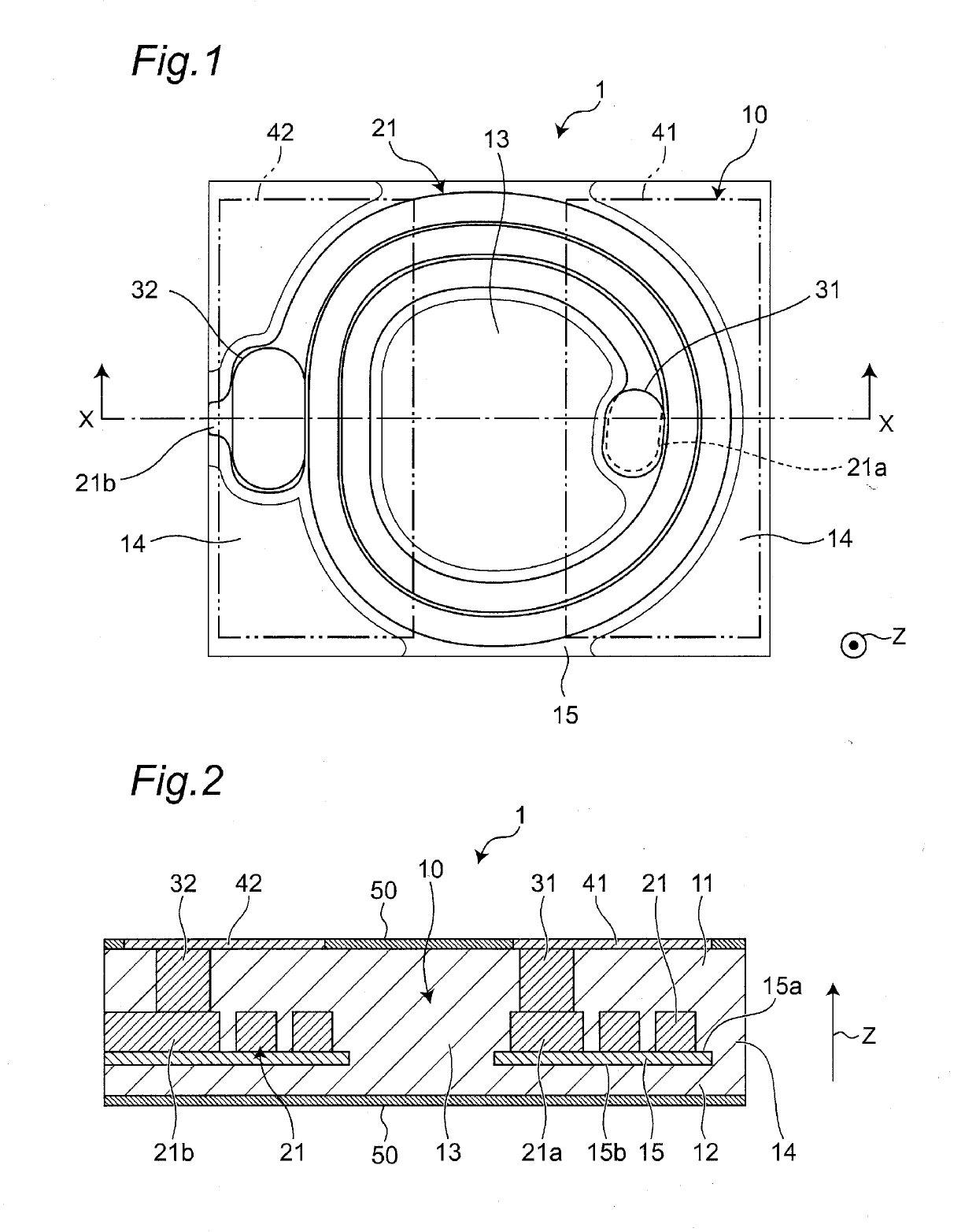
[0058]FIG. 1 is a transparent plan view of a first embodiment of an inductor component. FIG. 2 is a cross-sectional view taken along a line X-X of FIG. 1.
[0059]An inductor component 1 is mounted on an electronic device such as a personal computer, a DVD player, a digital camera, a TV, a portable telephone, and automotive electronics, for example, and is a component generally having a rectangular parallelepiped shape, for example. However, the shape of the inductor component 1 is not particularly limited and may be a circular columnar shape, a polygonal columnar shape, a truncated cone shape, or a truncated polygonal pyramid shape.
[0060]As shown in FIGS. 1 and 2, the inductor component 1 has a magnetic layer 10, an insulating layer 15, a spiral wiring 21, columnar wirings 31, 32, external terminals 41, 42, and a coating film 50.
[0061]The insulating layer 15 has a first principal surface 15a as an upper surface and a second principal surface 15b as a lower surface. A no...
example
[0112]An example of the inductor component 1 will be described.
[0113]The spiral wiring 21, the columnar wirings 31, 32, and the external terminals 41, 42 are made of low resistance metal such as Cu, Ag, and Au, for example. Preferably, the spiral wiring 21 with a low resistance and a narrow pitch can inexpensively be formed by using copper plating formed by SAP (semi additive process). The spiral wiring 21, the columnar wirings 31, 32, and the external terminals 41, 42 may be formed by a plating method other than SAP, a sputtering method, a vapor deposition method, an application method, etc.
[0114]In this example, the spiral wiring 21 and the columnar wirings 31, 32 are formed by copper plating with SAP, and the external terminals 41, 42 are formed by electroless Cu plating. The spiral wiring 21, the columnar wirings 31, 32, and the external terminals 41, 42 may all be formed by the same construction technique.
[0115]The magnetic layer 10 (the first magnetic layer 11, the second magn...
second embodiment
[0131]FIG. 4 is a cross-sectional view of a second embodiment of an inductor component. The second embodiment is different from the first embodiment in arrangement of the insulating layer. This different configuration will hereinafter be described. The other constituent elements have the same configuration as the first embodiment and are denoted by the same reference numerals as the first embodiment and will not be described.
[0132]As shown in FIG. 4, an inductor component 1A of the second embodiment has the spiral wiring 21 formed in a spiral shape exceeding one round. The side surface of the spiral wiring 21 is covered with the insulating layer 15 in a region where wirings run parallel to each other due to the spiral wiring 21 exceeding one round. In other words, the insulating layer 15 covers the lower surface of the spiral wiring 21 as in the first embodiment and further exists between the wirings of the spiral wiring 21 in the region exceeding one round. The thickness of the ins...
PUM
| Property | Measurement | Unit |
|---|---|---|
| thickness | aaaaa | aaaaa |
| size | aaaaa | aaaaa |
| thickness | aaaaa | aaaaa |
Abstract
Description
Claims
Application Information