
Random number generation
- Summary
- Abstract
- Description
- Claims
- Application Information
AI Technical Summary
Benefits of technology
Problems solved by technology
Method used
Image

Examples
Embodiment Construction
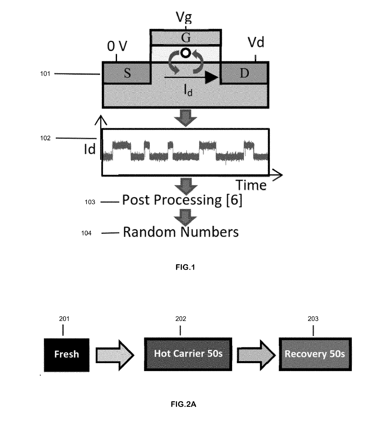
[0031]FIG. 1 illustrates an exemplary conventional method for true random number generation using Random Telegraph Noise (RTN) in semiconductor devices. In operation 101, the process of trapping / detrapping a single electron induces RTN. An RTN signal manifests itself in the form of drain voltage (Vd) or drain current (Id) fluctuations. Prior art methods rely on sampling the fluctuating signal (operation 102) and applying post-processing schemes (operation 103), such as the von Neumann algorithm, to de-bias the resulting signal. In operation 104, the de-biased signal is used to generate true random numbers.
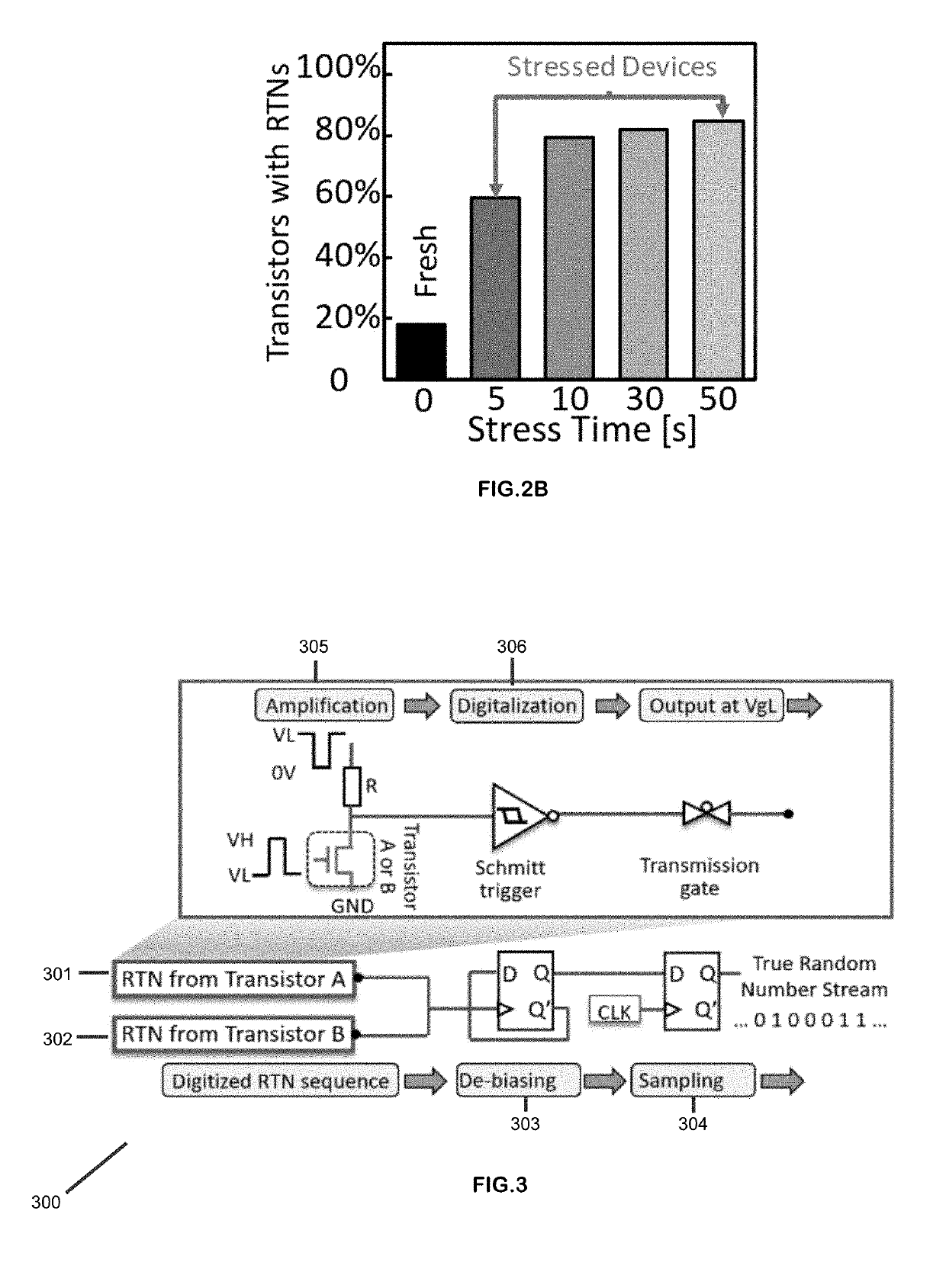
[0032]FIG. 2A illustrates the process of Random Telegraph Noise (RTN) generation using hot carrier stress in accordance with an embodiment of the present invention. The process involves exposing a fresh semiconductor device 201 to hot carrier stress for 50 seconds (operation 202). In operation 203, the device recovers for 50 seconds. As a result, a new trap can be generated. The ge...
PUM
 Abstract
Description
Claims
Application Information