Chip Package Structure And Packaging Method

a technology of chip package and packaging method, which is applied in the direction of semiconductor devices, electrical equipment, semiconductor/solid-state device details, etc., can solve the problems of not being beneficial to heat dissipation of chips, and not meeting requirements, so as to increase the bandwidth of top-layer chips, reduce the thickness of the package structure, and reduce the density of pins

Inactive Publication Date: 2019-09-05
HUAWEI TECH CO LTD
View PDF0 Cites 9 Cited by
  • Summary
  • Abstract
  • Description
  • Claims
  • Application Information

AI Technical Summary

Benefits of technology

[0106]In the chip package structure and packaging method in the embodiments of this application, the lower-layer substrate is replaced with the redistribution layer, so that the package structure thickness is reduced, the pin density is increased, the interconnection channel density is increased, and the bandwidth of the top-layer chip is increased.

Problems solved by technology

Consequently, this cannot meet a requirement for a smaller and thinner semiconductor package structure in a current technology, and is not beneficial to heat dissipation of the chip.

Method used


Image

  • Chip Package Structure And Packaging Method
  • Chip Package Structure And Packaging Method
  • Chip Package Structure And Packaging Method

Examples


Embodiment Construction

[0121]The following clearly describes the technical solutions in the embodiments of this application with reference to the accompanying drawings in the embodiments of this application.

[0122]For ease of understanding, first, a scenario that is applicable to a chip package structure in the embodiments of this application is simply described with reference to FIG. 1.

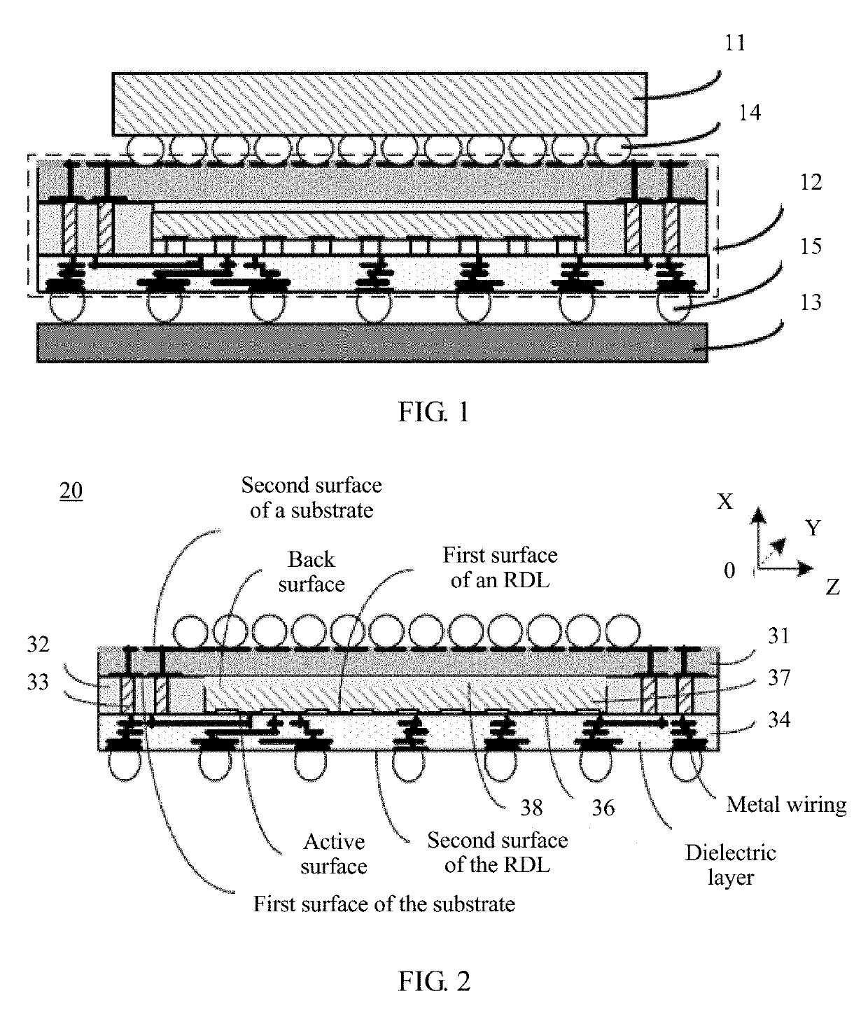
[0123]FIG. 1 is a schematic diagram of a scenario that is applicable to a chip package structure according to an embodiment of this application. As shown in FIG. 1, the chip package structure 12 may be connected to a top-layer chip 11 by using a connector 14 (for example, a weld ball, which may be specifically a solder ball (solder ball) or the like), and the chip package structure 12 may be connected to a lower-layer printed circuit board (Printed Circuit Board, PCB) 13 by using a connector 15 (for example, a weld ball, which may be specifically a solder ball or the like). The top-layer chip 11 may be a structure or a pack...


PUM


Abstract

Example chip package structure and packaging methods are described. One example chip package structure includes: a redistribution layer (RDL) and a target chip including an active surface and a back surface, where the active surface of the target chip is connected to a first surface of the RDL. The example chip package structure further includes a substrate, where a first surface of the substrate is opposite to the back surface of the target chip. The example chip package structure further includes an interconnection channel that is located around the target chip. One end of the interconnection channel is connected to the first surface of the RDL, and the other end of the interconnection channel is connected to the first surface of the substrate.

Description

CROSS-REFERENCE TO RELATED APPLICATIONS[0001]This application is a continuation of International Application No. PCT / CN2017 / 089188, filed on Jun. 20, 2017, which claims priority to Chinese Patent Application No. 201611028571.1, filed on Nov. 18, 2016, The disclosures of the aforementioned applications are hereby incorporated by reference in their entireties.TECHNICAL FIELD[0002]This application relates to the field of chip package, and more specifically, to a chip package structure and packaging method.BACKGROUND[0003]With a rapid increase of portable electronic products, a semiconductor package structure installed on a printed circuit board (PCB) in an electronic device is gradually smaller and thinner. Therefore, package becomes more important in an industry chain.[0004]Currently, in a known package structure, a chip is packaged between an upper-layer substrate and a lower-layer substrate by using a package on package (POP) technology. Specifically, the lower-layer substrate may b...

Claims


Application Information

Patent Timeline
Patent Type & Authority Applications(United States)
IPC IPC(8): H01L23/538H01L23/00H01L23/31H01L21/48H01L21/56H01L25/10H01L25/00
CPCH01L23/5389H01L2224/73253H01L23/5386H01L24/16H01L23/3128H01L24/32H01L24/73H01L21/4857H01L21/4853H01L21/568H01L25/105H01L25/50H01L2224/16227H01L2224/32225H01L23/5383H01L25/0657H01L24/19H01L2224/0401H01L2224/04105H01L2224/1132H01L2224/11334H01L2224/11462H01L2224/12105H01L2224/13147H01L2224/73204H01L2224/73267H01L2224/81005H01L2224/92225H01L2224/92244H01L2224/97H01L2225/1035H01L2225/1041H01L2225/1058H01L2225/107H01L2225/1094H01L2924/15192H01L2924/15311H01L2924/1533H01L2924/18161H01L2924/00014H01L2224/83H01L2224/81H01L2224/16225H01L2924/00
Inventor FU, HUILILI, HENGZHANG, XIAODONG
Owner HUAWEI TECH CO LTD
Why Eureka
Try Eureka