
Semiconductor device and processor control method

Active Publication Date: 2019-10-31
RENESAS ELECTRONICS CORP
View PDF0 Cites 1 Cited by
  • Summary
  • Abstract
  • Description
  • Claims
  • Application Information

AI Technical Summary

Benefits of technology

The patent text describes a semiconductor device that can reduce power consumption. The device monitors its use during a first term and adjusts the frequency of the clock signal supplied to the processor during a second term to achieve this goal. The result is a significant reduction in power consumption during the second term.

Problems solved by technology

Therefore, such a problem as increase in a power consumption of the processor is caused.
For example, a lot of industrial network apparatuses are placed in a factory, and such a problem as increase in an entire power consumption of the factory is also caused by the increase in the power consumptions of the processors of the industrial network apparatuses.
That is, also when the processor executes the idle task, it consumes the same power as a power consumed when it executes the higher-priority task.
Therefore, it cannot be said that the entire processing of the real-time OS is optimized, and there is a concern that the power consumption of the data processor cannot be reduced down to an expected value.
On the other hand, when a demanded performance not having the sufficient margin is set, there is a concern that the real-time task to be executed at a certain cycle cannot be entirely processed to lose the real-time performance.

Method used


Image

  • Semiconductor device and processor control method
  • Semiconductor device and processor control method
  • Semiconductor device and processor control method

Examples


first embodiment

[0023]

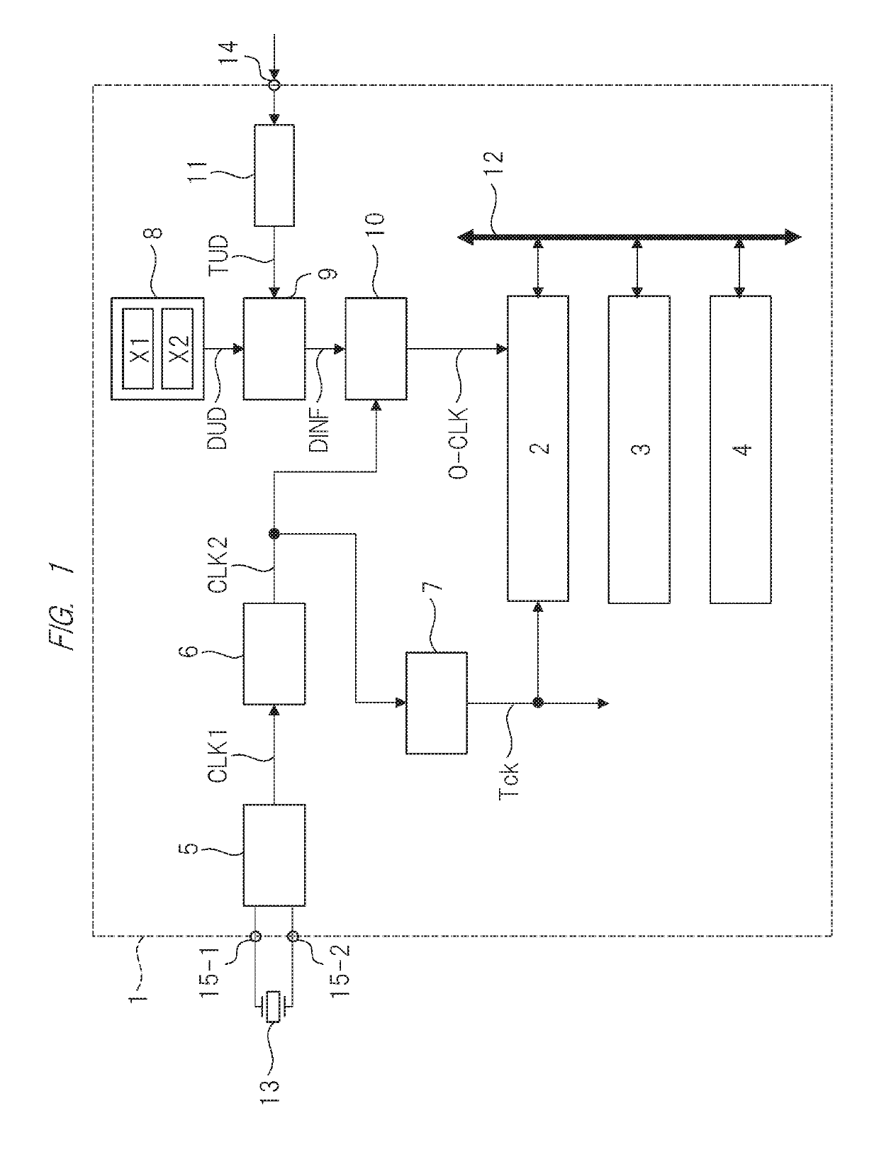
[0024]FIG. 1 is a block diagram showing a configuration of a semiconductor device according to a first embodiment. Although not particularly limited, a semiconductor device 1 shown in FIG. 1 is a semiconductor device for industrial network communication. While the semiconductor device 1 has a plurality of circuit blocks for the network communication, FIG. 1 shows only a portion required for explanation.

[0025]In FIG. 1, a numerical symbol “2” indicates a processor connected to a bus 12. To the bus 12, not only the processor 2 but also a plurality of peripheral blocks, memories and others are connected. In this drawing, as the peripheral block, a direct memory access controller (hereinafter, referred to as DMA controller) 3 is connected to the bus 12. And, a numerical symbol “4” indicates the memory connected to the bus 12. In the memory 4, a program of a real-time OS and a plurality of application programs operating on the real-time OS are stored.

[0026]The processor 2 reads out...

second embodiment

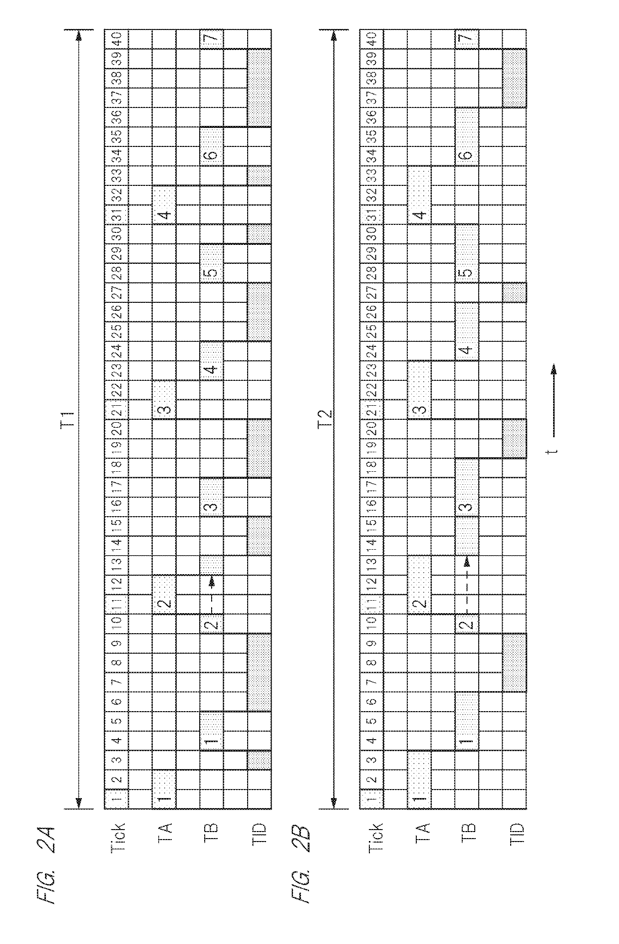
[0072]In a second embodiment, a semiconductor device capable of suppressing rapid change of the frequency of the operational clock signal is provided. In the first embodiment, the frequency dividing value is selected on the basis of the use rate of the processor measured during the first term T1 (in FIG. 2), and the frequency of the operational clock signal O-CLK supplied to the processor 2 during the second term T2 (in FIG. 2) is determined by the selected frequency dividing value. Therefore, in shift from the first term T1 to the second term T2, it is concerned that the frequency of the operational clock signal O-CLK largely changes. It is thought that a large change amount of the frequency of the operational clock signal O-CLK makes the operation of the processor 2 unstable. The second embodiment provides stepwise change in the frequency dividing value of which the frequency-dividing-value selecting circuit 9 (in FIG. 1) notifies the frequency dividing circuit 10. This manner can...


PUM


Abstract

A semiconductor device capable of reducing power consumption is provided. A semiconductor device having a processor executing a plurality of tasks while switching the tasks in synchronization with a supplied operational clock signal includes: a processor-use-rate measuring unit configured to measure a use rate of the processor during a first term; and a frequency-dividing-value selecting circuit and a frequency dividing circuit configured to change a frequency of the operational clock signal supplied to the processor during a second term later than the first term on the basis of the use rate measured by the processor-use-rate measuring unit.

Description

CROSS-REFERENCE TO RELATED APPLICATION[0001]The present application claims priority from Japanese Patent Application No. 2018-86891 filed on Apr. 27, 2018, the content of which is hereby incorporated by reference into this application.TECHNICAL FIELD OF THE INVENTION[0002]The present invention relates to a semiconductor device having a processor and to a processor control method. For example, the present invention relates to a semiconductor device having a processor executing a plurality of tasks while switching the tasks and to a processor control method.BACKGROUND OF THE INVENTION[0003]In order to allow a processor to execute a plurality of tasks while switching the tasks, a multitask operating system (hereinafter, referred to as “OS”) is operated on the processor, and the plurality of tasks are operated on the multitask OS. The tasks include a task required to be executed at a previously-determined certain cycle, that is, a task required to have a real-time performance (hereinaft...

Claims


Application Information

Patent Timeline
IPC IPC(8): G06F9/52G06F9/48G06F1/3203G06F1/08
CPCG06F9/4818G06F1/3203G06F9/52G06F1/08G06F1/3228G06F1/324G06F9/4893Y02D10/00
Inventor SHIMIZU, MASAYUKI
Owner RENESAS ELECTRONICS CORP
Features
  • Generate Ideas
  • Intellectual Property
  • Life Sciences
  • Materials
  • Tech Scout
  • Unparalleled Data Quality
  • Higher Quality Content
  • 60% Fewer Hallucinations
Learn More