Display device and method for manufacturing the same
a technology of display device and manufacturing method, which is applied in the direction of basic electric elements, semiconductor devices, electrical apparatus, etc., can solve the problems of difficult to embody those structures through a common formation method
- Summary
- Abstract
- Description
- Claims
- Application Information
AI Technical Summary
Benefits of technology
Problems solved by technology
Method used
Image
Examples
third embodiment
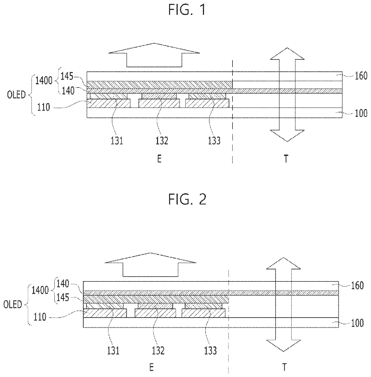
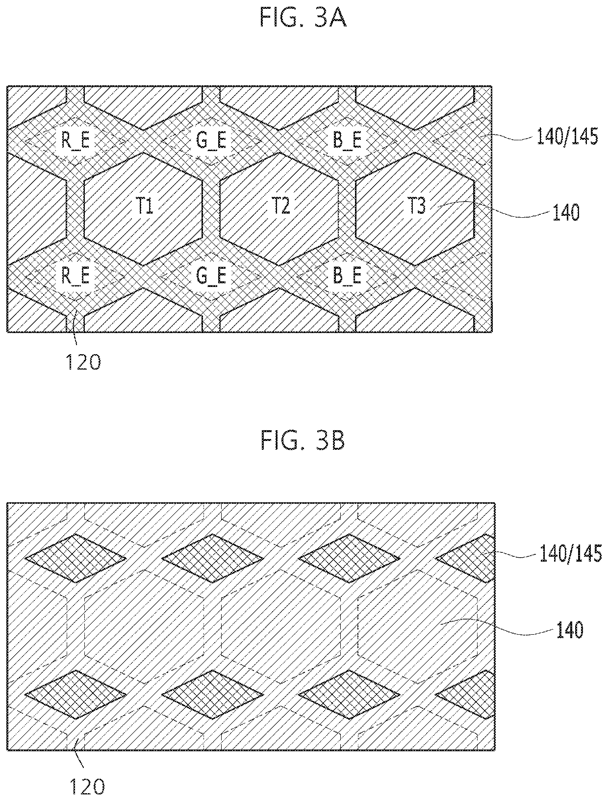
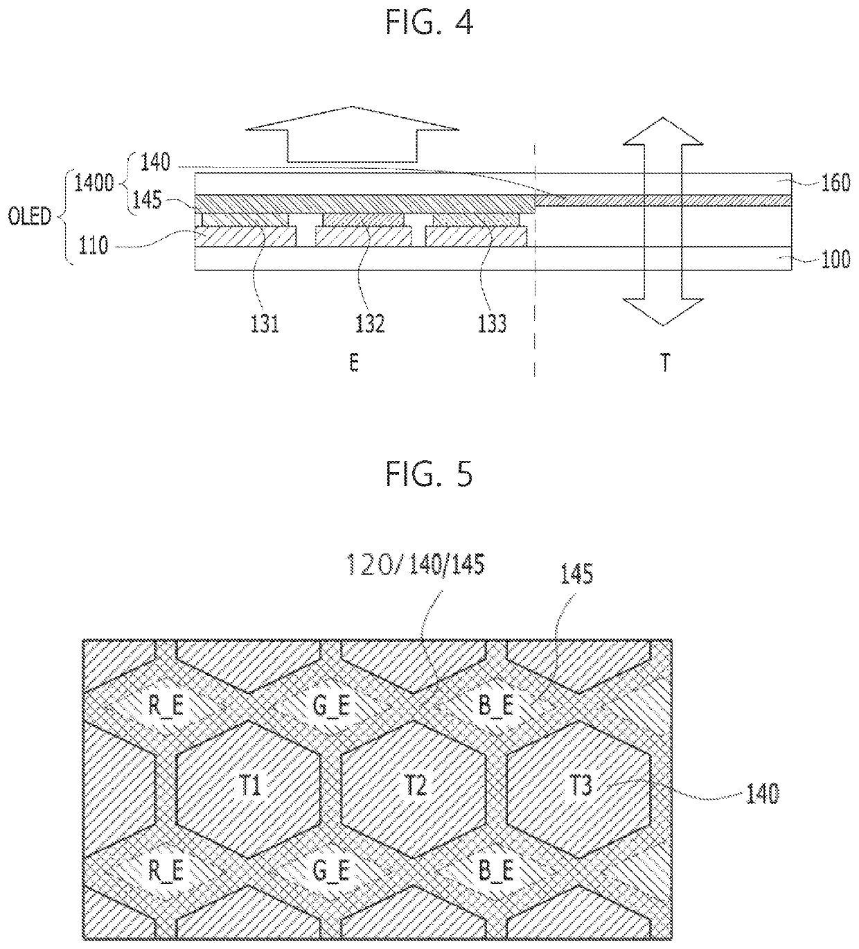
[0095]In the display device according to the present disclosure as described above, the transmissive electrode structure 1400 is constituted by forming the first layer 140 at the transmission parts T (Ti, T2 and T3) using a transparent metal in order to enhance transmissivity and forming the second layer 145 at the emission parts E (R_E, G_E and B_E) using a translucent metal or a translucent alloy such that the second layer 145 has a predetermined thickness, taking into consideration a cavity-based optimal resonance efficiency. The first layer 140 may be formed to have a thickness of 30 to 120 nm, using a transparent oxide containing at least one metal selected from indium (In), titanium (Ti), zinc (Zn) and tin (Sn). The second layer 145 may be formed to have a thickness of 10 to 27 nm, using a metal selected from Ag, Mg and Yb or an ally selected from an alloy of Ag and Mg, an alloy of Ag and Yb and an alloy of Ag, Mg and Yb.
[0096]The second layer 145 at the emission parts E has a...
second embodiment
[0129]FIGS. 9A to 9G are cross-sectional views illustrating a method for manufacturing the display device according to the present disclosure. FIGS. 10A and 10B are plan views illustrating examples of a mask used in a process for forming the second layer of the transmissive electrode structure. FIG. 11 is a plan view illustrating an example of a mask used in a process of FIG. 9F.
[0130]FIG. 9A illustrates a method for forming one thin film transistor TFT and one reflective electrode structure 110 in association with one emission part E (R_E) and one transmission part T (T1).
[0131]In accordance with the illustrated method, a buffer layer 102 is first formed over the substrate 100. Thereafter, a semiconductor layer 104 is formed on the buffer layer 102, to correspond to the emission part E, and a gate insulating film 105 is then formed over the entire upper surface of the resulting structure. A gate electrode 106 is subsequently formed on the gate insulating film 105, to overlap with a...
PUM
 Abstract
Description
Claims
Application Information


