A plasmonic device

a plasmonic device and surface technology, applied in the direction of measurement devices, instruments, scientific instruments, etc., can solve the problems of major bottlenecks in detection sensitivity, severe limitations, and obstacles in visualizing these structures in detail, and achieve the effect of improving linear and nonlinear raman scattering processes

Inactive Publication Date: 2019-12-26
XFOLD IMAGING OY
View PDF0 Cites 5 Cited by
  • Summary
  • Abstract
  • Description
  • Claims
  • Application Information

AI Technical Summary

Benefits of technology

[0038]The present invention offers advantages over the known prior art. The plasmonic nanostructured devices according to the invention have a predefined shape or dimensions, arrangement and pattern which results in the strong enhancement of a number of optical phenomena, such as reflectance, absorption, extraordinary optical transmission, linear and non

Problems solved by technology

This is an obstacle for visualizing these structures in detail.
In addition, sensitivity of detection is a major bottleneck: the number of molecules may be too small to be detected or only a small fraction of them can be detected.
These can be severely limiting factors, especially in live sample imaging, due to direct photodamage or phototoxic effects.
In addition temperature of the structures of the prior art surface plasmonic (SP) nanostructures ill

Method used


Image

  • A plasmonic device
  • A plasmonic device
  • A plasmonic device

Examples


Embodiment Construction

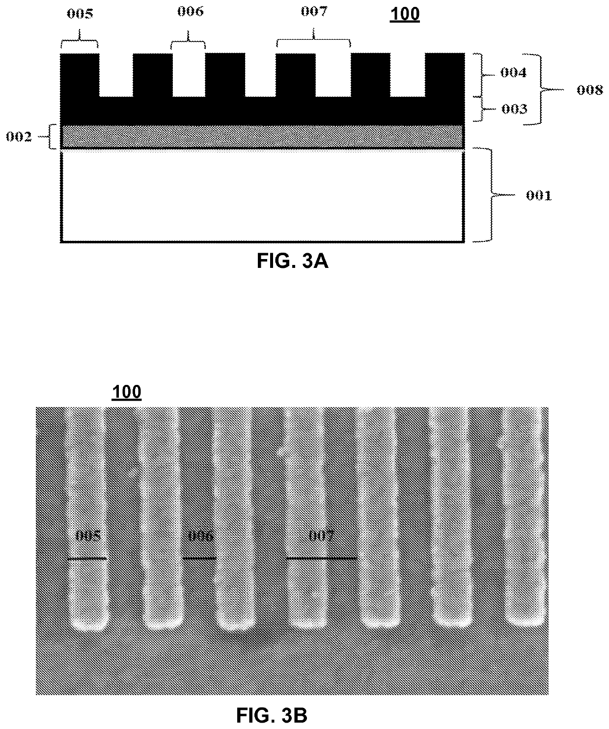
[0051]The different embodiments of plasmonic devices according to the invention are next described by referring to FIGS. 1-5.

[0052]The present invention is directed to surface plasmonic (SP) structures having well defined features at predetermined locations on a substrate for enhancing optical signal resulting from enhanced optical processes used in linear and nonlinear spectroscopy, microscopy and imaging techniques, such as SERS, SECARS and SRS.

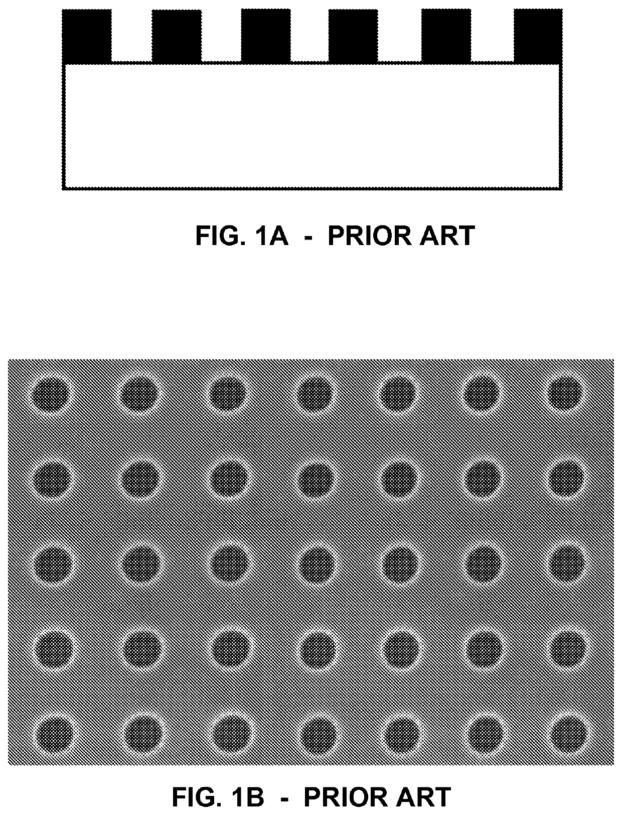
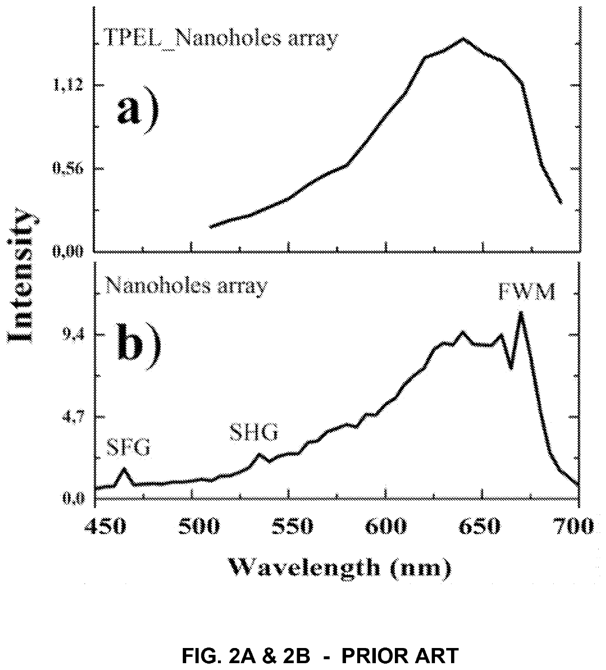
[0053]FIGS. 1A-1B and 2A-2B are already discussed in more details in the connection with the technical background chapter in this document.

[0054]An exemplary embodiment of the present invention of SP structures is shown in FIG. 3A. According to an embodiment of the invention the plasmonic device can be constructed in several ways, but it advantageously comprises at least one metal layer 003 and a 1-dimensional metal grating 004 consisting of metal stripes. Usually the device is constructed on some foreign substrate 001. The adhesive layer 0...


PUM


Abstract

A plasmonic device to enhance optical processes in samples lying on or in the proximity of the surface of the device comprises a substrate and a plasmonic structure. The plasmonic structure comprises advantageously a full metal layer and a metal grating in connection with the full metal layer. In addition the plasmonic device may comprise an optional adhesion layer between the substrate and the plasmonic structure and/or, an optional protective layer above the full metal layer or metal grating.

Description

TECHNICAL FIELD OF THE INVENTION[0001]The invention relates to surface plasmonic (SP) devices to enhance optical processes in samples in the proximity of the device. In particular, the invention relates to design and fabrication of plasmonic devices for linear and nonlinear microscopy and spectroscopy applications in physics, chemistry, biology, bioimaging and medical diagnostics field, for example.BACKGROUND OF THE INVENTION[0002]Many optical measurement techniques are nowadays used to image or characterize materials, structures, cells and tissue e.g. in physics, chemistry and biology. In many of these techniques the sample to be studied is placed on or in the proximity of the surface of a suitable substrate material. Many techniques also use light with known properties, such as laser light with a defined wavelength. To advance the state of the art in these case, the substrate on which the sample is placed, could contain some functionality to enhance the measurement process, such a...

Claims


Application Information

Patent Timeline
IPC IPC(8): G02B5/00
CPCG02B5/008G02B5/1809G01N21/554
Inventor SUBRAMANIYAM, NAGARAJANSOPANEN, MARKKUIKONEN, ELINAISOMÄKI, ANTTIPFISTERER, SIMON
Owner XFOLD IMAGING OY
Why Eureka
Try Eureka