Dynamic imaging system

Active Publication Date: 2020-01-16
APPLIED MATERIALS INC
View PDF8 Cites 3 Cited by
  • Summary
  • Abstract
  • Description
  • Claims
  • Application Information

AI Technical Summary

Benefits of technology

The patent describes a system for manufacturing electronic devices. The system includes a slab, a moveable stage, a first encoder, an inspection system, and a digital lithography support. The inspection system can measure the shape of the substrate and the position of any dies on it without exposing the substrate to the process. This data is used to create a compensated pattern that is sent to the digital lithography system. The digital lithography system then uses this compensated pattern to expose the substrate and create the desired electronic device. The technical effect of this system is to improve the accuracy and efficiency of the manufacturing process.

Problems solved by technology

One issue encountered in any lithography process involving large area display panel substrates and small area semiconductor substrates exposed to back-end processing is substrate warpage.
This results in the eventual production of a lower quality, or even a non-functional, display panel, and advance package product.

Method used


Image

  • Dynamic imaging system
  • Dynamic imaging system
  • Dynamic imaging system

Examples


Embodiment Construction

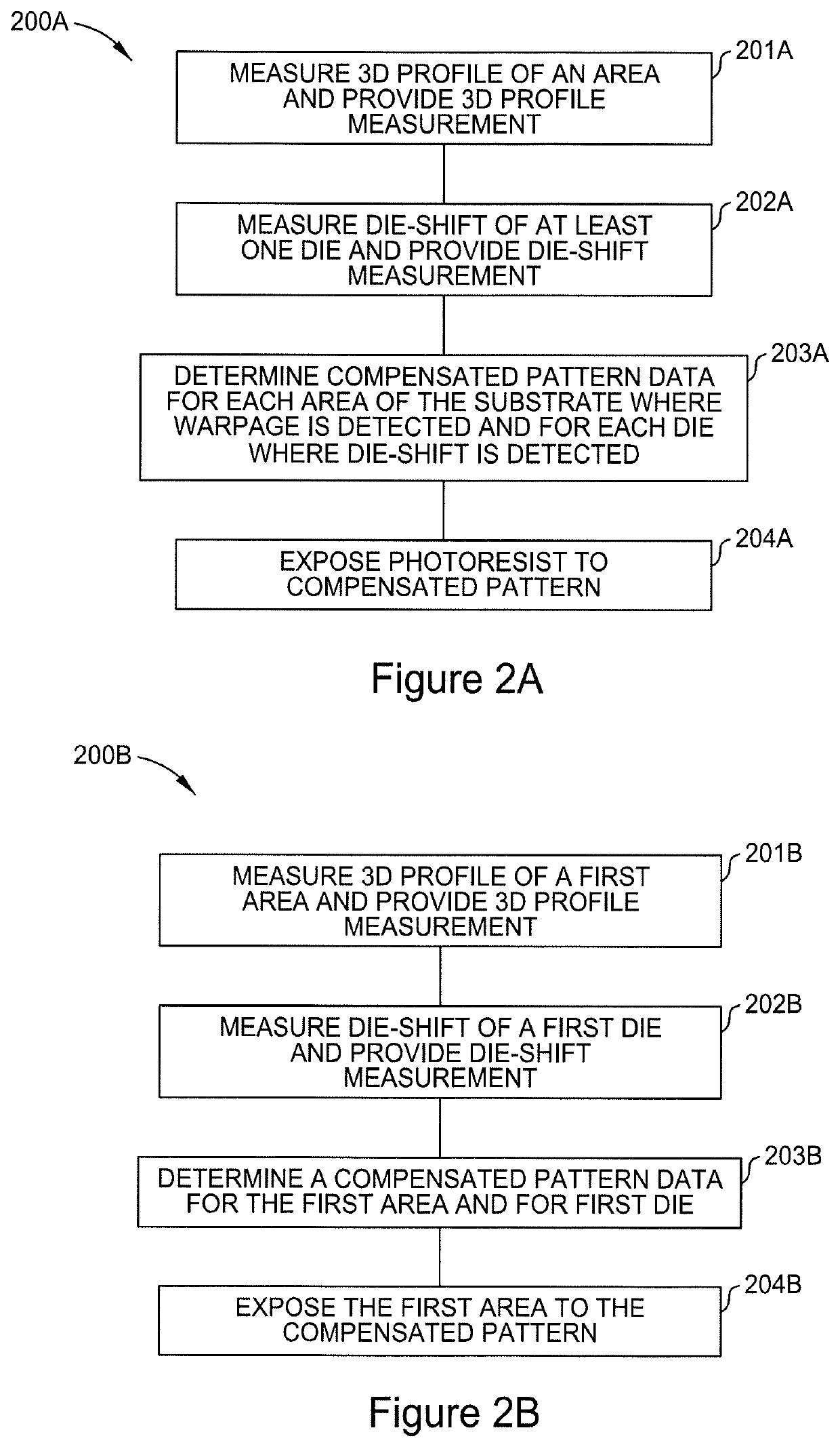
[0021]Embodiments described herein provide dynamic imaging systems that compensates for pattern defects resulting from distortion caused by warpage and die-shift. Herein, the methods and apparatus described are useful to create compensated exposure patterns in photoresists, or other written to film layers, wherein later changes in the dimensions of the substrate result in the proper positioning of the exposure pattern, and any resultant etched film layer. For example, where a substrate is warped and at least on die is shifted during the lithography process, the system and methods herein allow a digital exposure pattern to be written to a photoresist on a substrate compensating for warpage and die-shift.

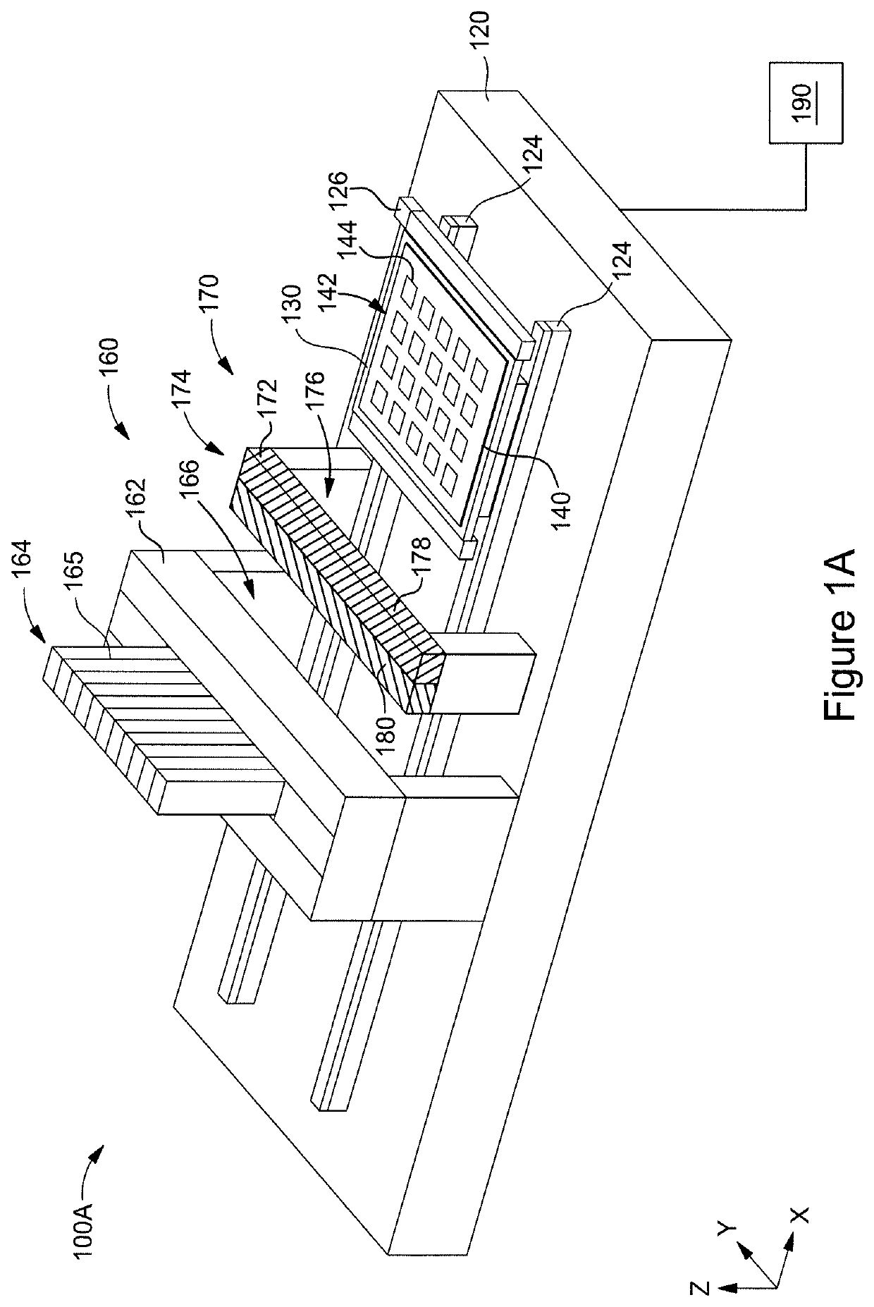
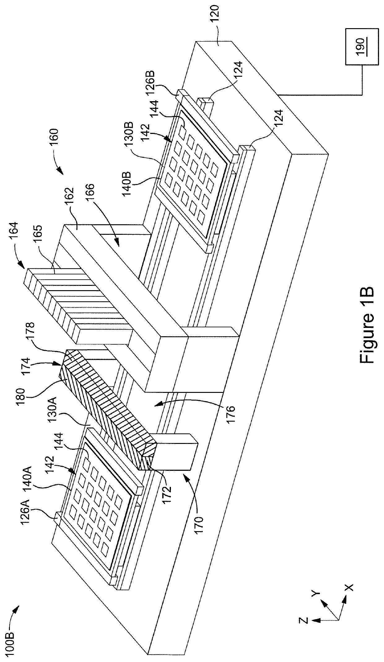
[0022]FIG. 1A is a perspective schematic view of a dynamic imaging system 100A according to embodiments disclosed herein. The dynamic imaging system 100A includes a stage 130, a digital lithography system 160, and an inspection system 170. In one embodiment, the stage 130 is supported...


PUM


Abstract

Embodiments described provide dynamic imaging systems that compensates for pattern defects resulting from distortion caused by warpage of the substrate. The methods and apparatus described are useful to create compensated exposure patterns. The dynamic imaging system includes an inspection system configured to provide 3D profile measurements and die shift measurements of the first substrate to the interface configured to provide compensated pattern data to the digital lithography system configured to receive the compensated pattern data from the interface and expose the photoresist with a compensated pattern.

Description

BACKGROUNDField[0001]Embodiments of the present disclosure generally relate to photolithography systems. More particularly, embodiments of the present disclosure relate to digital lithography systems that compensate for pattern defects.Description of the Related Art[0002]Photolithography is widely used in the manufacturing of semiconductor devices, such as for back-end processing of semiconductor devices, and display devices, such as liquid crystal displays (LCDs). For example, large area substrates are often utilized in the manufacture of LCDs. LCDs, or flat panel displays, are commonly used for active matrix displays, such as computers, touch panel devices, personal digital assistants (PDAs), cell phones, television monitors, and the like. Generally, flat panel displays include a layer of liquid crystal material as a phase change material at each pixels, sandwiched between two plates. When power from a power supply is applied across or through the liquid crystal material, an amoun...

Claims


Application Information

Patent Timeline
IPC IPC(8): G03F7/20
CPCG03F7/7065G03F7/70291G03F7/703G03F7/70508G03F9/7003
Inventor CHEN, CHING-CHANGLAI, CHIEN-HUACHEN, WEI-CHUNGKUO, SHIH-HAOWANG, HSIU-JEN
Owner APPLIED MATERIALS INC
Why Eureka
Try Eureka