
Semiconductor Device

Active Publication Date: 2020-01-16
AMS AG
View PDF2 Cites 3 Cited by
  • Summary
  • Abstract
  • Description
  • Claims
  • Application Information

AI Technical Summary

Benefits of technology

The present patent provides a semiconductor device with increased efficiency. By arranging several contact layers at different vertical positions, it is possible to electrically contact different parts of the semiconductor device without consuming more area of the device by forming other electrical contacts or vias. The contact layer can be electrically connected with other parts of the semiconductor device by arranging several contact layers at different vertical positions. The formation of cracks can be avoided since the lateral extent in the first lateral direction of the contact layer is smaller than the lateral size of the via. The semiconductor device can be operated more efficiently. The semiconductor device also includes an electrically conductive top contact which can extend over a part of the lateral extent of the semiconductor device. The contact layer can be structured with a grid-like pattern to decrease the probability of crack formation. The lateral extent in a second lateral direction of at least one of the contact layer is larger than the lateral extent in the second lateral direction of the via to minimize the area where the metal is in contact with the non-conductive material and the probability of cracks occurring.

Problems solved by technology

Because of this difference in the coefficients of thermal expansion, it is possible that during processing of the semiconductor device cracks occur in or around the contact material of the through silicon via or in one of the metal layers.
These cracks can lead to leakage currents or it is possible that dirt or humidity can enter the semiconductor device.

Method used


Image

  • Semiconductor Device
  • Semiconductor Device

Examples


Embodiment Construction

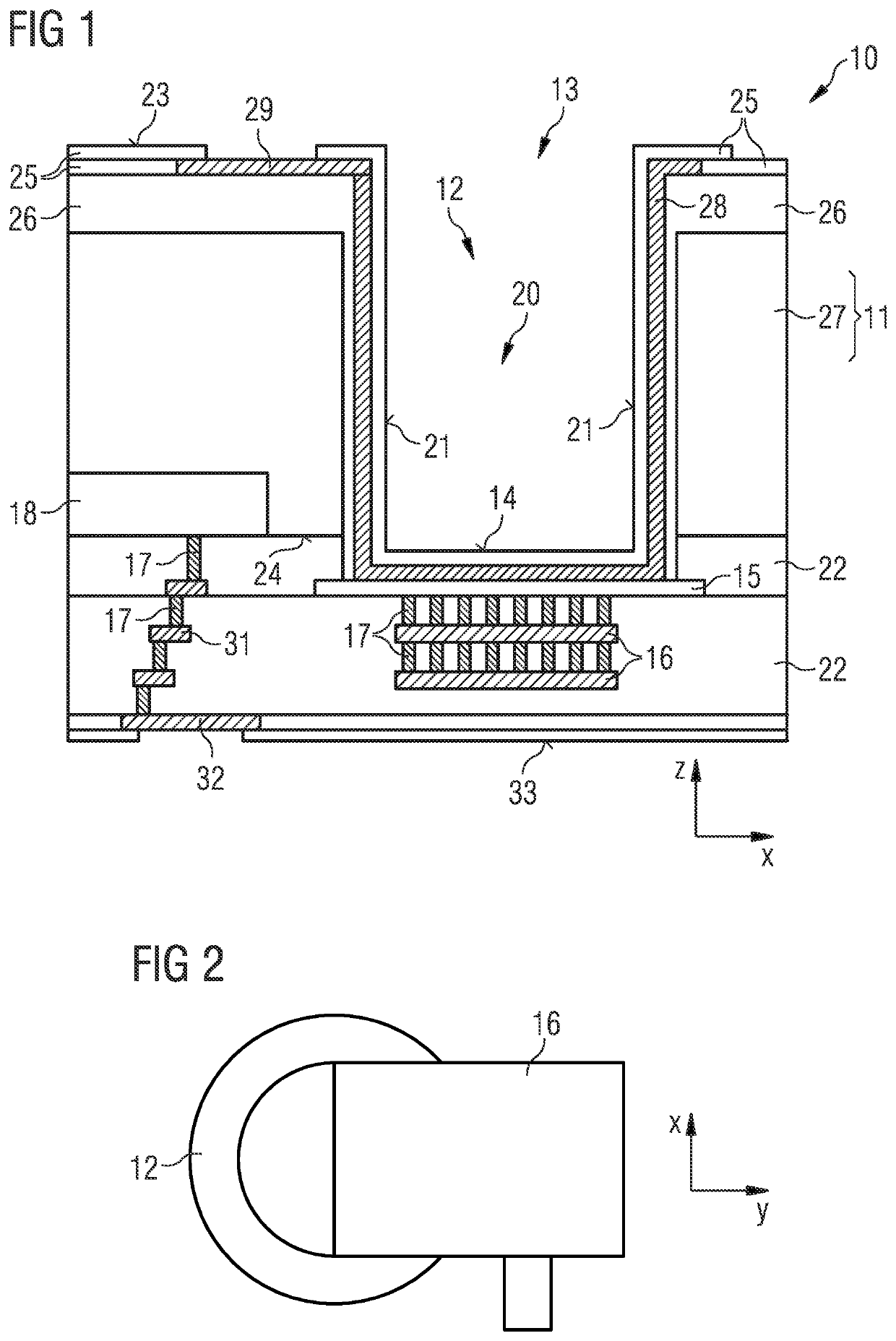
[0034]In FIG. 1, a cutaway view of an exemplary embodiment of a semiconductor device 10 is shown. The semiconductor device 10 comprises a semiconductor body 11. The semiconductor body 11 comprises a substrate 27. The substrate 27 can, for example, comprise silicon. Furthermore, an electrically non-conductive material 22 is arranged on the substrate 27 at a circuit side 24 of the semiconductor body 11. Within the non-conductive material 22, other materials such as metals are arranged. Moreover, at the circuit side 24 of the semiconductor body 11 an integrated circuit 18 is arranged.

[0035]An electrically conductive via 12 extends through the semiconductor body 11 and a part of the non-conductive material 22. The via 12 has a main axis of extension which is perpendicular to the main plane of extension of the substrate 27. This means the main axis of extension of the via 12 is parallel to a vertical direction z which is perpendicular to the main plane of extension of the substrate 27. T...


PUM


Abstract

A semiconductor device comprises a semiconductor body and an electrically conductive via which extends through at least a part of the semiconductor body, where the via has a lateral size which is given in a first lateral direction that is perpendicular to a vertical direction given by the main axis of extension of the via and where the via has a top side and a bottom side that faces away from the top side. The semiconductor device further comprises an electrically conductive etch-stop layer arranged at the bottom side of the via in a plane which is parallel to the first lateral direction, and at least one electrically conductive contact layer at the bottom side of the via in a plane which is parallel to the first lateral direction. The lateral extent in the first lateral direction of the etch-stop layer is larger than the lateral size of the via and the lateral extent in the first lateral direction of the contact layer is smaller than the lateral size of the via. Furthermore, the etch-stop layer is arranged between the electrically conductive via and the contact layer in the vertical direction.

Description

CROSS-REFERENCE TO RELATED APPLICATIONS[0001]The present application is the national stage entry of International Patent Application No. PCT / EP2018 / 053694, filed on Feb. 14, 2018, which claims the benefit of priority of European Patent Application No. 17156319.0, filed on Feb. 15, 2017, all of which are hereby incorporated by reference in their entirety for all purposes.[0002]The present application relates to a semiconductor device.BACKGROUND OF THE INVENTION[0003]In order to electrically contact an integrated circuit of a semiconductor device or another part of a semiconductor device, a common method is to form a through silicon via through the silicon substrate of the device. Therefore, a trench is formed in the substrate. The trench is at least partially filled with an electrically conductive contact material and the contact material is electrically isolated against the substrate. An integrated circuit which is arranged at a circuit side of the substrate can be electrically cont...

Claims


Application Information

Patent Timeline
IPC IPC(8): H01L23/48H01L23/528H01L23/00
CPCH01L2224/06181H01L24/06H01L2224/0557H01L24/05H01L23/481H01L23/528H01L23/522
Inventor KRAFT, JOCHENPARTEDER, GEORGSINGULANI, ANDERSONCOPPETA, RAFFAELESCHRANK, FRANZ
Owner AMS AG
Features
  • Generate Ideas
  • Intellectual Property
  • Life Sciences
  • Materials
  • Tech Scout
  • Unparalleled Data Quality
  • Higher Quality Content
  • 60% Fewer Hallucinations
Learn More