Solid-state image capture device and image capture device

a technology of image capture device and image capture device, which is applied in the direction of semiconductor/solid-state device details, radio-controlled devices, television systems, etc., can solve the problems of reducing pixel array b>1021/b>, and difficulty in achieving both an increase in imaging area and a downsizing of the chip, so as to increase the area ratio of imaging area and reduce the chip size. , the effect of increasing the proportion of imaging

Active Publication Date: 2020-02-20
NUVOTON TECH CORP JAPAN
View PDF0 Cites 2 Cited by
  • Summary
  • Abstract
  • Description
  • Claims
  • Application Information

AI Technical Summary

Benefits of technology

[0015]In view of the above-described problem, it is an object of the present disclosure to provide a solid-state image capture device and an image capture device that can achieve both an increase in the area of imaging area, which increases the proportion of the imaging area to the chip size, and a downsizing of the chip.
[0018]The solid-state image capture device and the image capture device according to the present disclosure can achieve both an increase in the area ratio of imaging area, which increases the proportion of the imaging area of the chip size, and a downsizing of the chip.

Problems solved by technology

The above-described conventional technique, however, has a problem in that as the chip size decreases, the proportion of pad areas 1221 and 1222 to first chip 1020 increases and the area ratio of the imaging area, i.e., pixel array 1021, decreases.
In other words, it is difficult to achieve both an increase in the area ratio of imaging area and a downsizing of the chip.
That is, it is difficult to increase the number of pixels.
However, when the configuration of the solid-state imaging device disclosed in PTL 1 is used, it is difficult to ensure a region for TSVs because circuitry (second chip) is disposed under the pads (first chip) in a stacked sensor in which first chip 1020 and second chip 1030 are stacked.
That is, the pads on the first chip cannot be connected to solder balls provided on the rear face of a mount board on which a stacked body of the first chip and the second chip is mounted.
Thus, the above-described configuration cannot use CSP technology.
In order to achieve the aforementioned connection, it is necessary to ensure a region for TSVs, and this inevitably increases the chip size.

Method used


Image

  • Solid-state image capture device and image capture device
  • Solid-state image capture device and image capture device
  • Solid-state image capture device and image capture device

Examples


embodiment 1

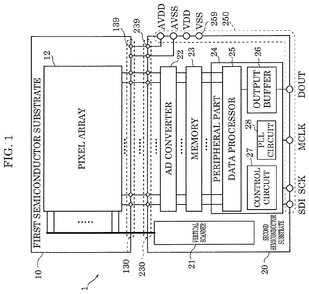
[0050]FIG. 1 is a block diagram illustrating a configuration example of solid-state image capture device 1 according to Embodiment 1.

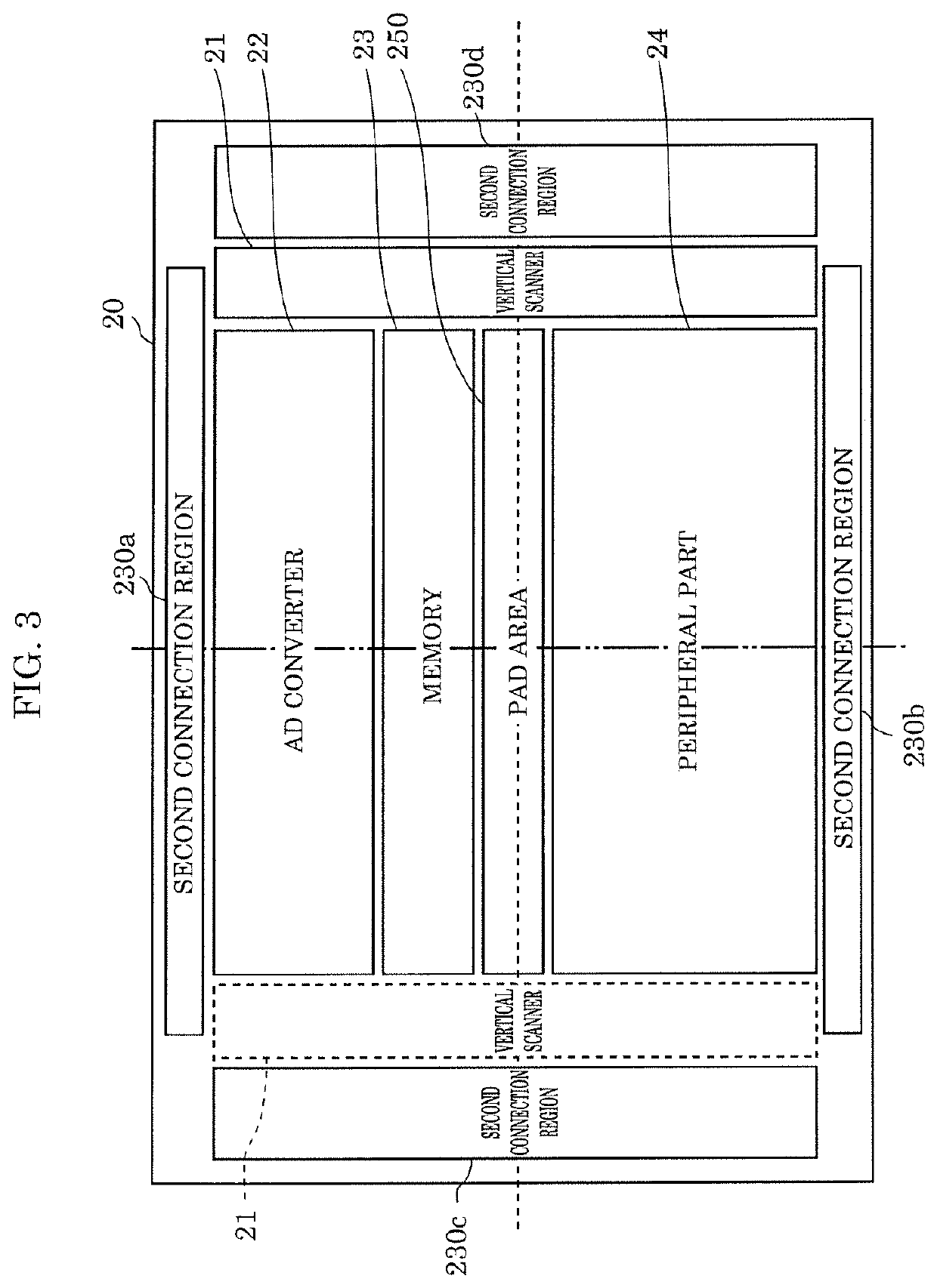
[0051]In FIG. 1, solid-state image capture device 1 includes first semiconductor substrate 10 (also referred to as a first chip) and second semiconductor substrate 20 (also referred to as a second chip). First semiconductor substrate 10 includes pixel array 12 and first connection 130. Second semiconductor substrate 20 includes vertical scanner 21, AD converter 22, memory 23, peripheral part 24, second connection 230, and pad area 250 (also referred to as a PAD).

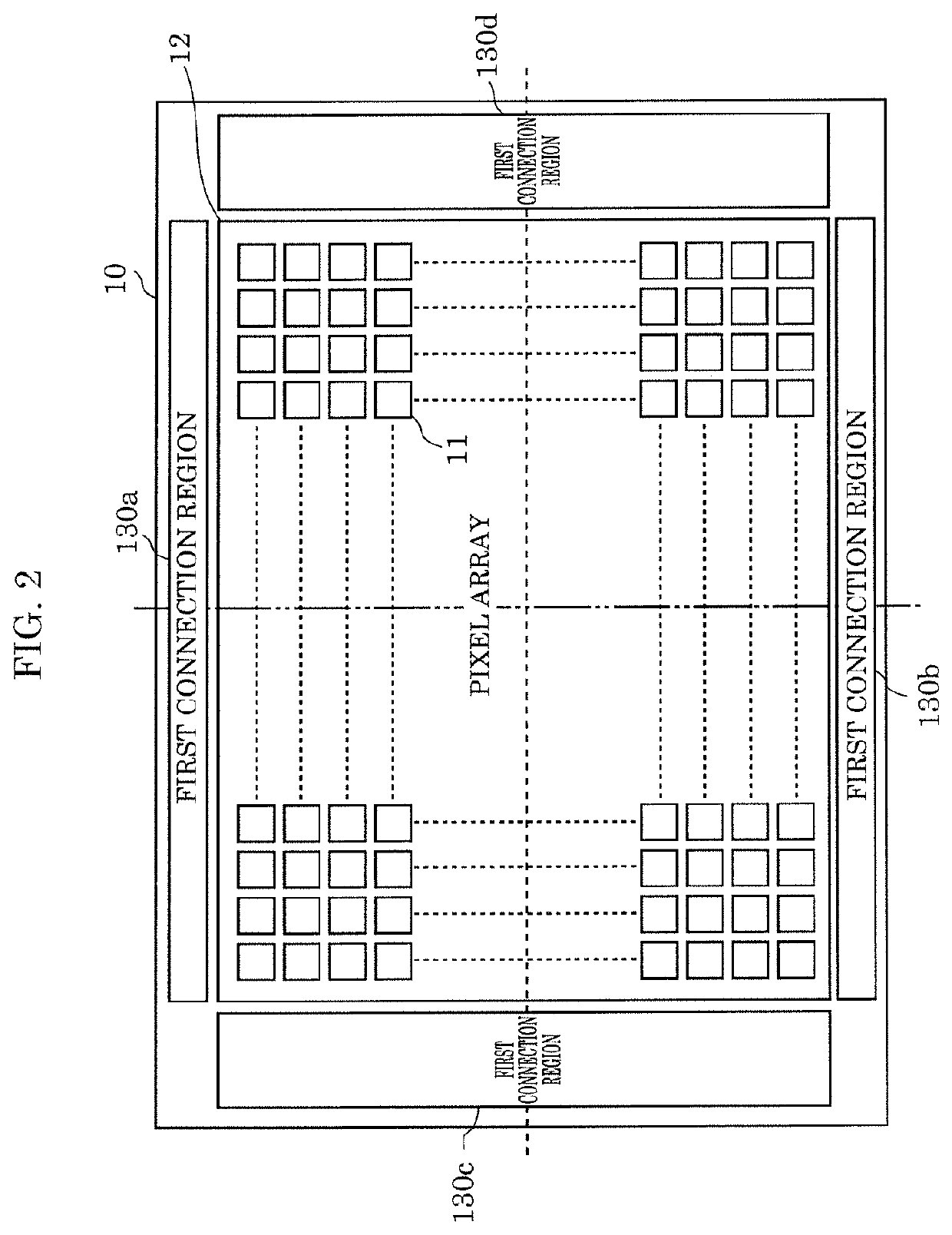
[0052]In first semiconductor substrate 10, pixel array 12 includes a plurality of pixels 11 arranged in a matrix.

[0053]First connection 130 includes a plurality of first connection electrodes 139 for transmitting signals received from pixel array 12. First connection electrodes 139 are connected to a rear face out of the two faces (front and rear faces) of first semiconductor substrate 10 so as...

embodiment 2

[0140]FIG. 8 illustrates a configuration example of solid-state image capture device 1 according to Embodiment 2. Compared to FIG. 1, solid-state image capture device 1 in FIG. 8 differs in that vertical scanner 21 is included in first semiconductor substrate 10, instead of being included in second semiconductor substrate 20. The following description focuses on the different point.

[0141]While vertical scanner 21 according to Embodiment 1 supplies various scanning signals to pixel array 12 via second connection 230 and first connection 130, vertical scanner 21 according to Embodiment 2 supplies various scanning signals directly to pixel array 12. Accordingly, the total number of first connection electrodes 139 in first connection 130 in FIG. 8 is smaller than the total number in FIG. 1. Similarly, the total number of second connection electrodes 239 in second connection 230 in FIG. 8 is smaller than the total number in FIG. 1.

[0142]FIG. 9 illustrates layout example 1 of first semico...

embodiment 3

[0157]FIG. 14 illustrates a configuration example of solid-state image capture device 1 according to Embodiment 3. Compared to FIG. 8, solid-state image capture device 1 in FIG. 14 differs in that AD converter 22 is eliminated and that first AD converter circuit 22A and second AD converter circuit 22B are additionally provided. The following description focuses on the different points.

[0158]First AD converter circuit 22A and second AD converter circuit 22B are circuits obtained by dividing AD converter 22 into two parts. That is, first AD converter circuit 22A corresponds to some circuits in AD converter 22 in FIG. 8, and second AD converter circuit 22B corresponds to the remaining circuits in AD converter 22.

[0159]For example, first AD converter circuit 22A corresponds to some analog functions of AD converter 22 in FIG. 8 and includes constant-current supply circuits for each pixel column, which are necessary to read out signals from pixels 11.

[0160]Second AD converter circuit 22B ...


PUM

PropertyMeasurementUnit
areaaaaaaaaaaa
sizeaaaaaaaaaa
speedaaaaaaaaaa

Abstract

A solid-state image capture device includes a first semiconductor substrate and a second semiconductor substrate. The first semiconductor substrate includes a first connection and a pixel array in which a plurality of pixels are arranged in a matrix. The second semiconductor substrate includes a second connection and a pad area including a plurality of pad electrodes for electrical connection with external equipment. The second semiconductor substrate controls the pixel array. The first and second semiconductor substrates are stacked and joined together, with the first and second connections electrically connected to each other. The first and second semiconductor substrates are substantially equal in size, and the pad electrodes are included in only the second semiconductor substrate.

Description

CROSS REFERENCE TO RELATED APPLICATIONS[0001]This application is a U.S. continuation application of PCT International Patent Application Number PCT / JP2018 / 015409 filed on Apr. 12, 2018, claiming the benefit of priority of Japanese Patent Application Number 2017-086176 filed on Apr. 25, 2017, the entire contents of which are hereby incorporated by reference.BACKGROUND1. Technical Field[0002]The present disclosure relates to a solid-state image capture device and an image capture device.2. Description of the Related Art[0003]A solid-state imaging device according to a conventional technique disclosed in WO 2014 / 007004 (PTL 1) will be described hereinafter with reference to FIG. 26. Referring to FIG. 26, solid-state imaging device 1010A has a so-called stacked structure that includes first chip 1020 and second chip 1030 as semiconductor substrates, with first chip 1020 stacked on the upper side and second chip 1030 stacked on the lower side.[0004]First chip 1020 includes pixel array 10...

Claims


Application Information

Patent Timeline
Patent Type & Authority Applications(United States)
IPC IPC(8): H04N5/369H01L27/146H04N5/3745H01L25/065H01L23/498
CPCH01L27/14636H04N5/379H01L27/14634H01L25/0657H04N5/37455H01L23/49816H01L27/14609H01L21/3205H01L21/768H01L23/522H01L27/14605H04N25/76H04N25/79H04N25/772
Inventor SHIMIZU, YUUSUKEONOZAWA, KAZUTOSHI
Owner NUVOTON TECH CORP JAPAN
Why Eureka
Try Eureka