Solid-state imaging device

a solid-state imaging and imaging device technology, applied in the direction of radio-controlled devices, transistors, television systems, etc., can solve the problem of limited area or the shape of the arranged photodiodes, and achieve the effect of preventing crosstalk and color mixing

Inactive Publication Date: 2020-03-05
OLYMPUS CORP
View PDF0 Cites 5 Cited by
  • Summary
  • Abstract
  • Description
  • Claims
  • Application Information

AI Technical Summary

Benefits of technology

[0016]According to the solid-state imaging device of each aspect described above, it is possible to provide a solid-state imaging device capable of p

Problems solved by technology

Furthermore, in the configuration of the pixel array of Patent Document 1, since it is necessary to arrange the transistor inside

Method used


Image

  • Solid-state imaging device
  • Solid-state imaging device
  • Solid-state imaging device

Examples


first embodiment

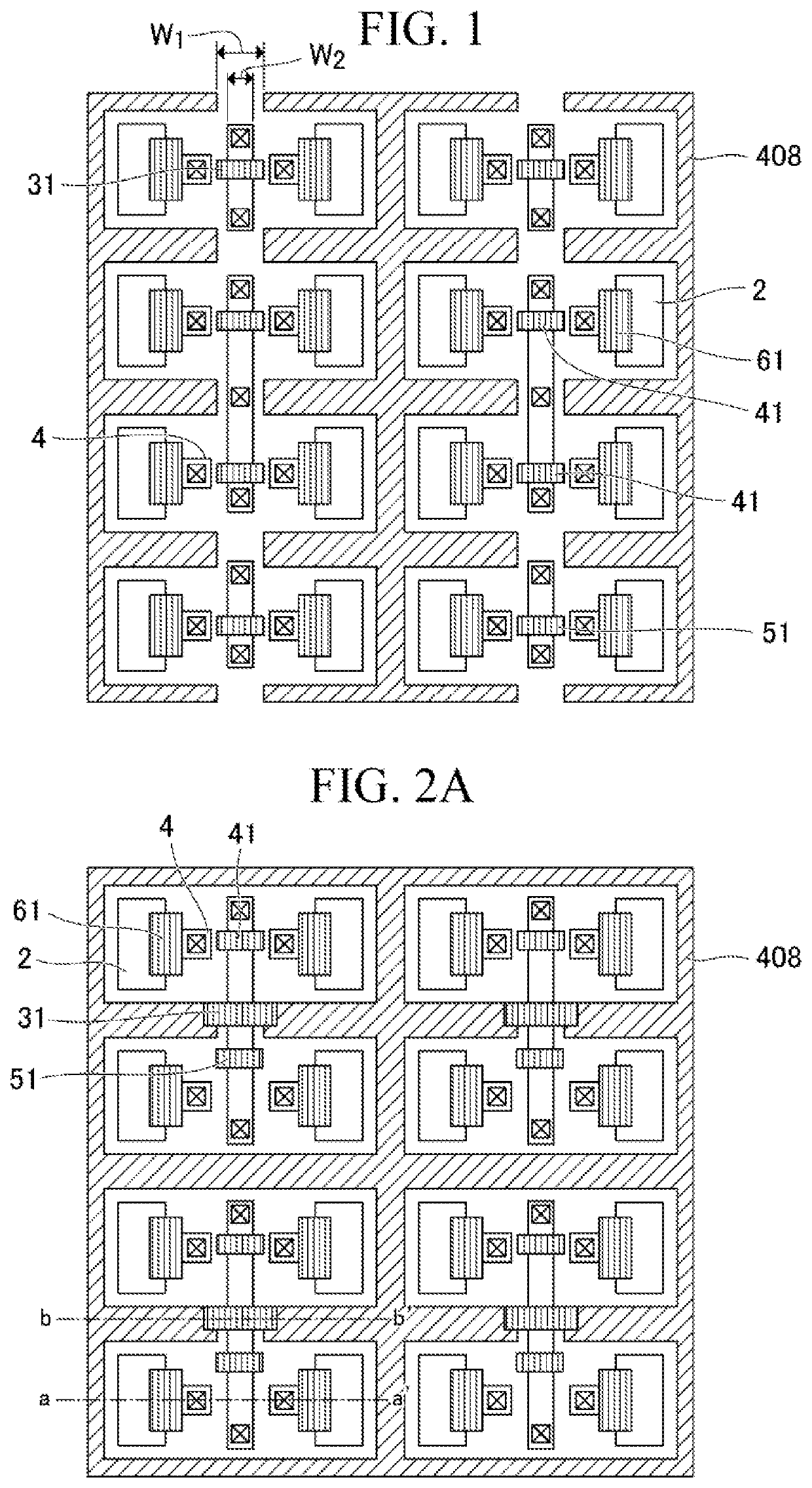
[0025]A first embodiment of the present invention will be described. FIG. 1 is a plan view showing a configuration of a pixel array in the solid-state imaging device according to the first embodiment of the present invention. In the pixel array, unit pixels are two-dimensionally arranged on the semiconductor substrate 404. In FIG. 1, 16 unit pixels of “4 pixels in the horizontal direction”ד4 pixels in the vertical direction” are arranged.

[0026]The element isolation insulating film (element isolation region) 408 is formed of an insulating film having a refractive index lower than that of the silicon layer of the semiconductor substrate. In Patent Document 1, the element isolation insulating film 408 is provided at all boundary portions between adjacent unit pixels on the semiconductor substrate. However, in the first embodiment of the present invention, as shown in FIG. 1, among the element isolation insulating film 408 surrounding each unit pixel, the element isolation insulating f...

second embodiment

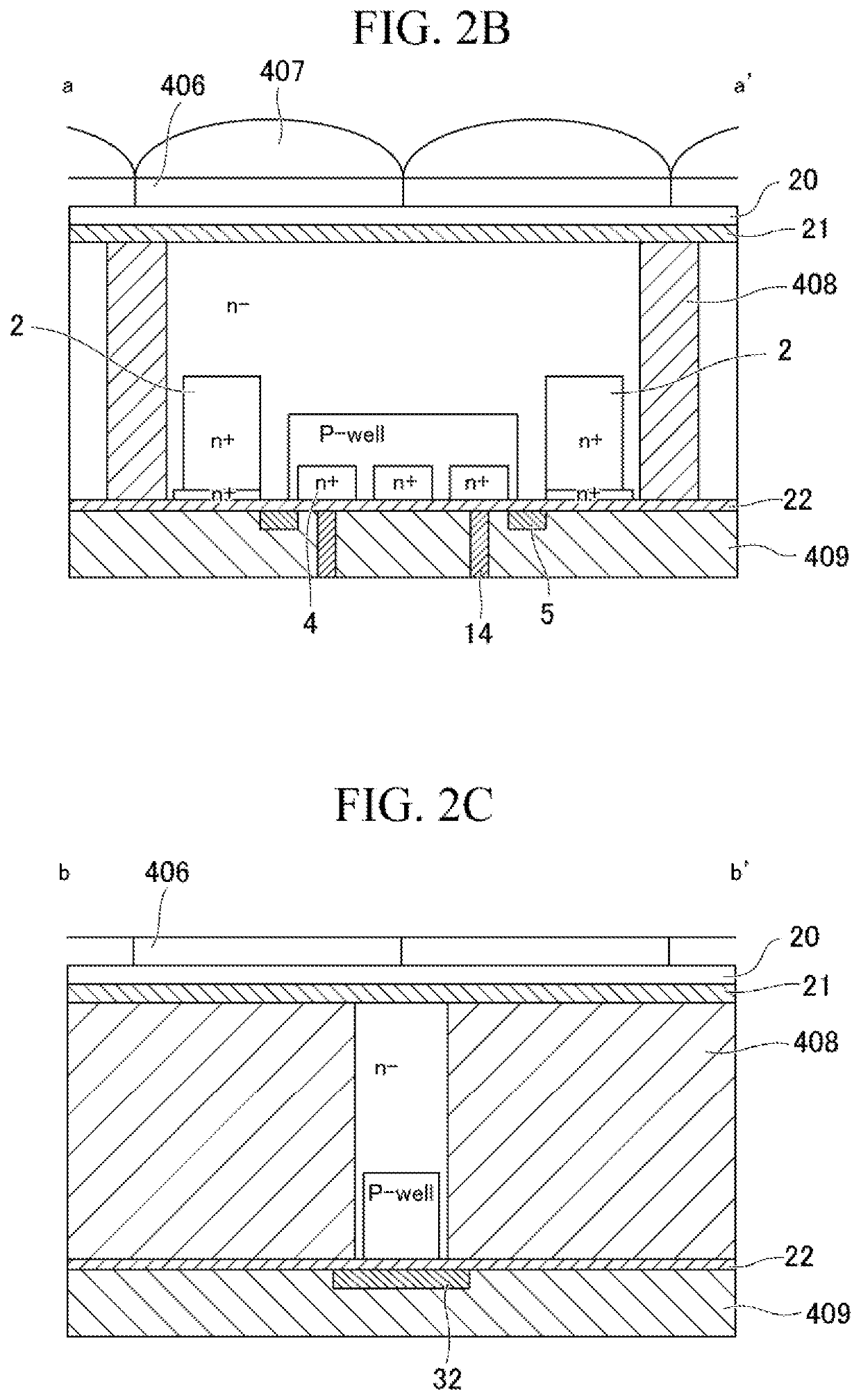
[0036]A second embodiment of the present invention will be described. FIG. 2A is a plan view showing the configuration of the pixel array in the solid-state imaging device according to the second embodiment of the present invention. As in FIG. 1, in the pixel array, unit pixels are two-dimensionally arranged on the semiconductor substrate 404, and 16 unit pixels of “4 pixels in the horizontal direction”ד4 pixels in the vertical direction” are arranged.

[0037]A difference from the configuration in FIG. 1 is that in FIG. 2A, four unit pixels of “2 pixels in the horizontal direction”ד2 pixels in the vertical direction” share various transistors. Therefore, as shown in FIG. 2A, among the element isolation insulating films 408 surrounding each unit pixel, the element isolation insulating film 408 of one side that separates adjacent unit pixels and the element isolation insulating film 408 positioned above or below the one side are omitted.

[0038]Also in the configuration of FIG. 2A, the ...

third embodiment

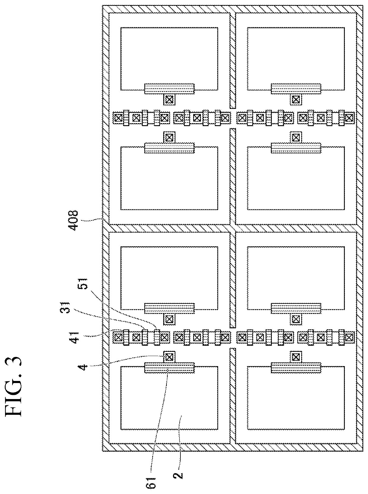
[0050]A third embodiment of the present invention will be described. FIG. 3 is a plan view showing the configuration of the pixel array in the solid-state imaging device according to the third embodiment of the present invention. In FIG. 3, in the pixel array, unit pixels are two-dimensionally arranged on the semiconductor substrate 404, and eight unit pixels of “2 pixels in the horizontal direction”ד4 pixels in the vertical direction” are arranged. The form of the element isolation insulating film 408 in the configuration of FIG. 3 is the same as the form of the element isolation insulating film 408 in FIG. 2A.

[0051]The difference from the configuration of FIG. 2A is that in the configuration of FIG. 3, various transistors and their active areas are not shared between unit pixels. In the configuration of FIG. 3, various transistors other than the transfer transistor 61 and their active areas are arranged in the vertical direction at intermediate portions of the floating diffusions...


PUM


Abstract

A solid-state imaging device includes a two-dimensional pixel array in which unit pixels are arranged on a semiconductor substrate, each including a photoelectric conversion element, and a circuit element. When a plurality of adjacent unit pixels are defined as one pixel group set, a plurality of pixel group sets are arranged in the two-dimensional pixel array. In the one pixel group set, a periphery of the one pixel group set is surrounded by an insulating element isolation region that isolates elements in the semiconductor substrate, except for an intermediate portion between two adjacent unit pixels. In the one pixel group set, two adjacent photoelectric conversion elements are arranged so that two floating diffusions respectively connected to the two adjacent photoelectric conversion elements are opposed to each other with the circuit element interposed therebetween. A transistor shared by the one pixel group set is provided in the intermediate portion.

Description

CROSS REFERENCE TO RELATED APPLICATIONS[0001]This application is a continuation application based on a PCT Patent Application No. PCT / JP2017 / 018015, filed on May 12, 2017, the content of which is incorporated herein by reference.BACKGROUNDTechnical Field[0002]The present invention relates to a solid-state imaging device. More specifically, the present invention relates to a solid-state imaging device in which a plurality of unit pixels are arranged in a two-dimensional matrix on a semiconductor substrate.Background Art[0003]In general, in a solid-state imaging device or an image sensor, signal charges generated and accumulated by photoelectric conversion elements of pixels on which light is incident are guided to an amplifying unit provided in the pixel, and a signal amplified by the amplifying unit is output from the pixel. Some solid-state imaging devices and image sensors using a semiconductor substrate include a pixel array in which a plurality of unit pixels are arranged in a t...

Claims


Application Information

Patent Timeline
IPC IPC(8): H01L27/146H04N5/369
CPCH01L27/14612H01L27/14643H01L27/14641H04N5/379H01L27/1463H01L27/14621H01L31/02H01L27/14603H01L27/1464H01L27/1461H01L27/14627H04N25/134H04N25/79
Inventor AOKI, JUNKOYAMA, YUSAKU
Owner OLYMPUS CORP
Why Eureka
Try Eureka