
Patsnap Eureka
For R&D, Patsnap Eureka makes reading and utilizing patents & technical documents easy.
Patsnap Eureka AIR
Designed for self-driven R&D workflows. Generate viable solutions, solve complex R&D challenges, empower your innovation with AI.

Patsnap Eureka Materials
Designed for material experts only. Revolutionize your material R&D, from search, analyze, to developing new materials.

TechResearch
Generate reliable direction feasibility study reports for your R&D in just a few steps.

TechSeek
Discover and master advanced knowledge NOW. Basics, ideas, possibilities, all at once.

TechMind
As an expert in R&D Theories, TechMind can generates customized viable solutions instantly.

TechRisk
Analyze your overall solution with one click, know your potential R&D risks in advance.

TechMonitor
Get weekly tech updates, stay abreast of the latest tech innovations and key insights.
Nonvolatile memory devices and methods of operating a nonvolatile memory
a nonvolatile memory and non-volatile technology, applied in the field of semiconductor memory devices, can solve the problems of reducing the read margin of flash memory, affecting the performance of flash memory, and including error bits in data read from memory cells, so as to reduce the errors in read data and enhance the performance of on-chip performance
- Summary
- Abstract
- Description
- Claims
- Application Information
AI Technical Summary
Benefits of technology
Problems solved by technology
Method used
Image

Examples
Embodiment Construction
[0036]Various example embodiments will be described more fully hereinafter with reference to the accompanying drawings, in which some example embodiments are shown.
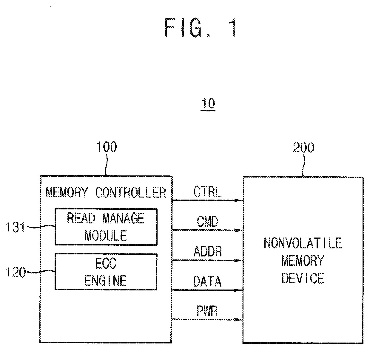
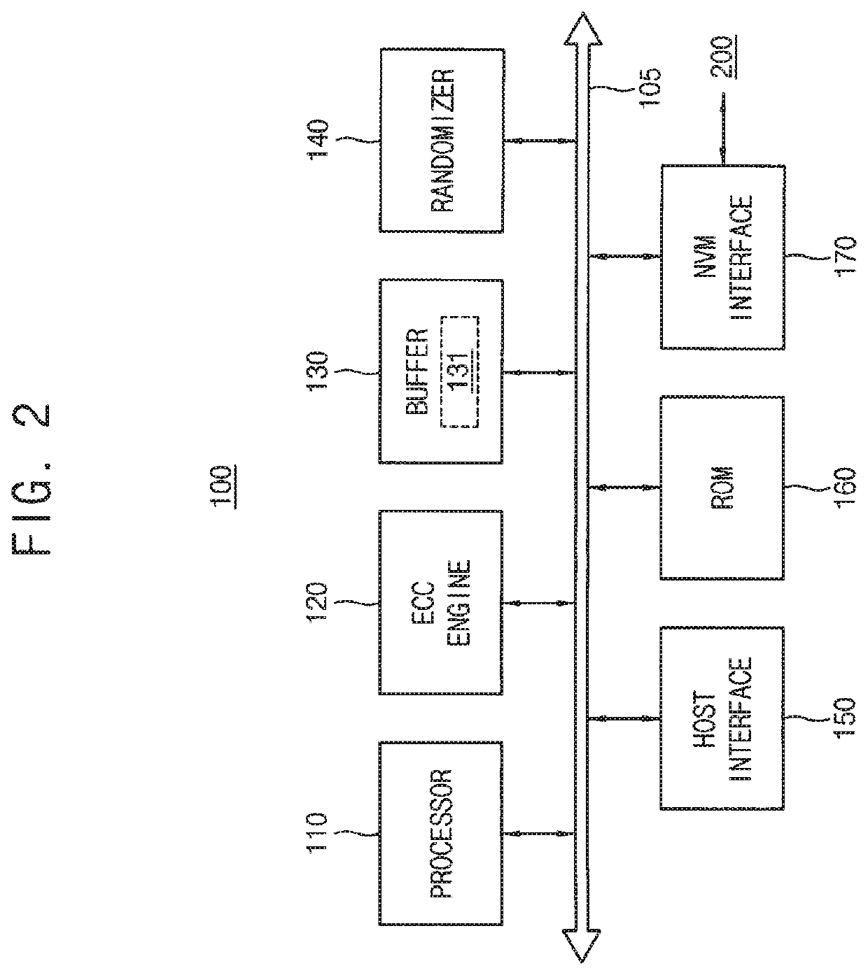
[0037]FIG. 1 is a block diagram illustrating a memory system 10 (e.g., a storage device) the according to example embodiments.
[0038]Referring to FIG. 1, a storage device (e.g., a memory system) 10 may include a memory controller 100 and at least one nonvolatile memory device 200.
[0039]In example embodiments, each of the memory controller 100 and the nonvolatile memory device 200 may be provided with the form of a chip, a package, and / or a module. Alternatively, the memory controller 100 and the nonvolatile memory device 200 may be packaged together into one of various packages. According to some example embodiments, the memory controller 100 and / or control elements of the nonvolatile memory device 200 may be implemented using processing circuitry. The term “processing circuitry,” as used in the present disclosure, may ref...
PUM
 Abstract
Description
Claims
Application Information
 - R&D Engineer
- R&D Manager
- IP Professional
- Industry Leading Data Capabilities
- Powerful AI technology
- Patent DNA Extraction
Browse by: Latest US Patents, China's latest patents, Technical Efficacy Thesaurus, Application Domain, Technology Topic, Popular Technical Reports.
© 2024 PatSnap. All rights reserved.Legal|Privacy policy|Modern Slavery Act Transparency Statement|Sitemap|About US| Contact US: help@patsnap.com