
Voltage-enhanced-feedback sense amplifier of resistive memory and operating method thereof

a resistive memory and amplifier technology, applied in the direction of information storage, static storage, digital storage, etc., can solve the problems of limiting the access time of the memory, reading failure, and bottlenecking the development time of the sensing operation, and achieve the effect of enhancing voltage difference and voltage differen

Active Publication Date: 2020-04-02
NATIONAL TSING HUA UNIVERSITY
View PDF0 Cites 5 Cited by
  • Summary
  • Abstract
  • Description
  • Claims
  • Application Information

AI Technical Summary

Benefits of technology

The present disclosure describes a voltage-enhanced-feedback sense amplifier of a resistive memory that is configured to sense a first bit line and a second bit line. The amplifier includes a voltage sense amplifier and a voltage-enhanced-feedback pre-amplifier. The voltage-enhanced-feedback pre-amplifier includes a first bit-line amplifying module and a second bit-line amplifying module. The amplifier is designed to enhance the margin of the voltage difference between the first and second bit lines, and the margin is greater than the read voltage difference. The operating method of the amplifier involves applying multiple voltage levels to the first and second bit lines, and amplifying the voltage levels using the amplifier to generate output signals. The technical effect of the present disclosure is to improve the accuracy and reliability of the resistive memory by enhancing the margin of the voltage difference between the first and second bit lines.

Problems solved by technology

However, sensing margin time of the memory is the key factor which may limit the access time of the memory.
In a long bit-line length resistive memory array, developing time would be a bottleneck in sensing operation since it takes lots of time to accumulate a slow-growing voltage difference between a bit-line voltage and a reference voltage.
Decreasing of developing time leads to read failure because the voltage difference between the bit-line voltage and the reference voltage is smaller than an offset voltage from the sense amplifier.
Furthermore, when a resistance value of a resistive type memory is low, the bit lines drop quickly to a ground voltage, and the sensing time of the resistive type memory will be easily affected by a bit line length, so that a small voltage difference between the bit lines is produced to cause low sensing yield and low sensing speed.

Method used


Image

  • Voltage-enhanced-feedback sense amplifier of resistive memory and operating method thereof
  • Voltage-enhanced-feedback sense amplifier of resistive memory and operating method thereof
  • Voltage-enhanced-feedback sense amplifier of resistive memory and operating method thereof

Examples


Embodiment Construction

[0020]Before describing any embodiments in detail, some terms used in the following are described. A voltage level of “1” represents that the voltage is equal to a power supply voltage VDD. The voltage level of “0” represents that the voltage is equal to a ground voltage VSS. A PMOS transistor and an NMOS transistor represent a P-type MOS transistor and an N-type MOS transistor, respectively. Each transistor has a source, a drain and a gate.

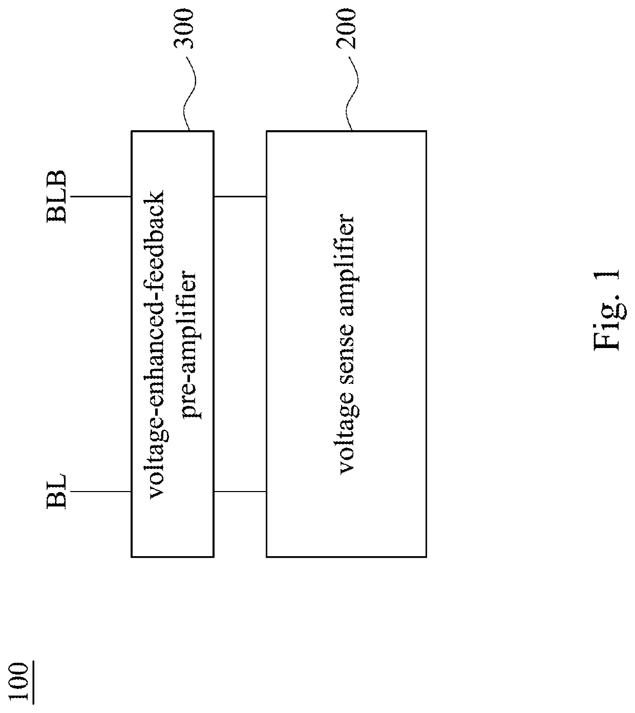
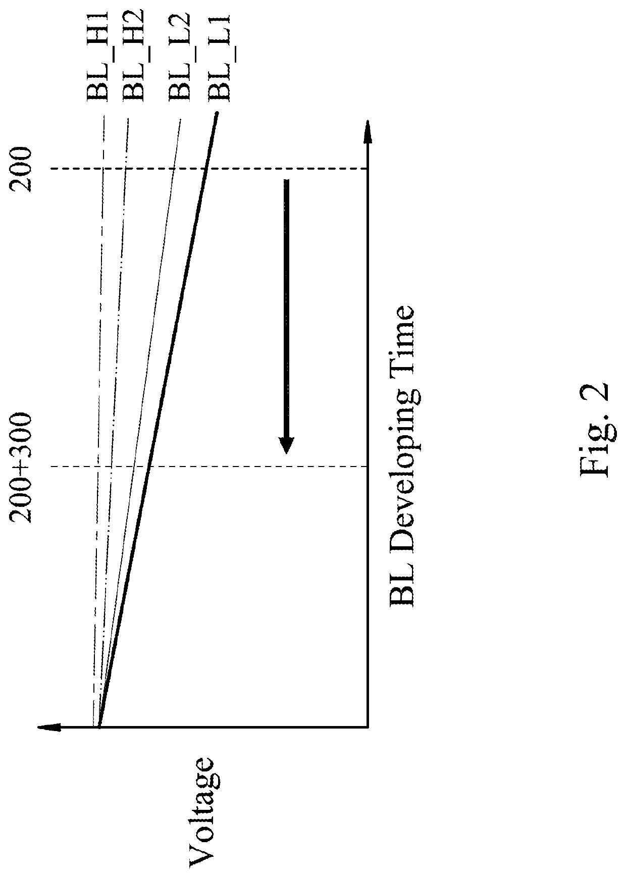
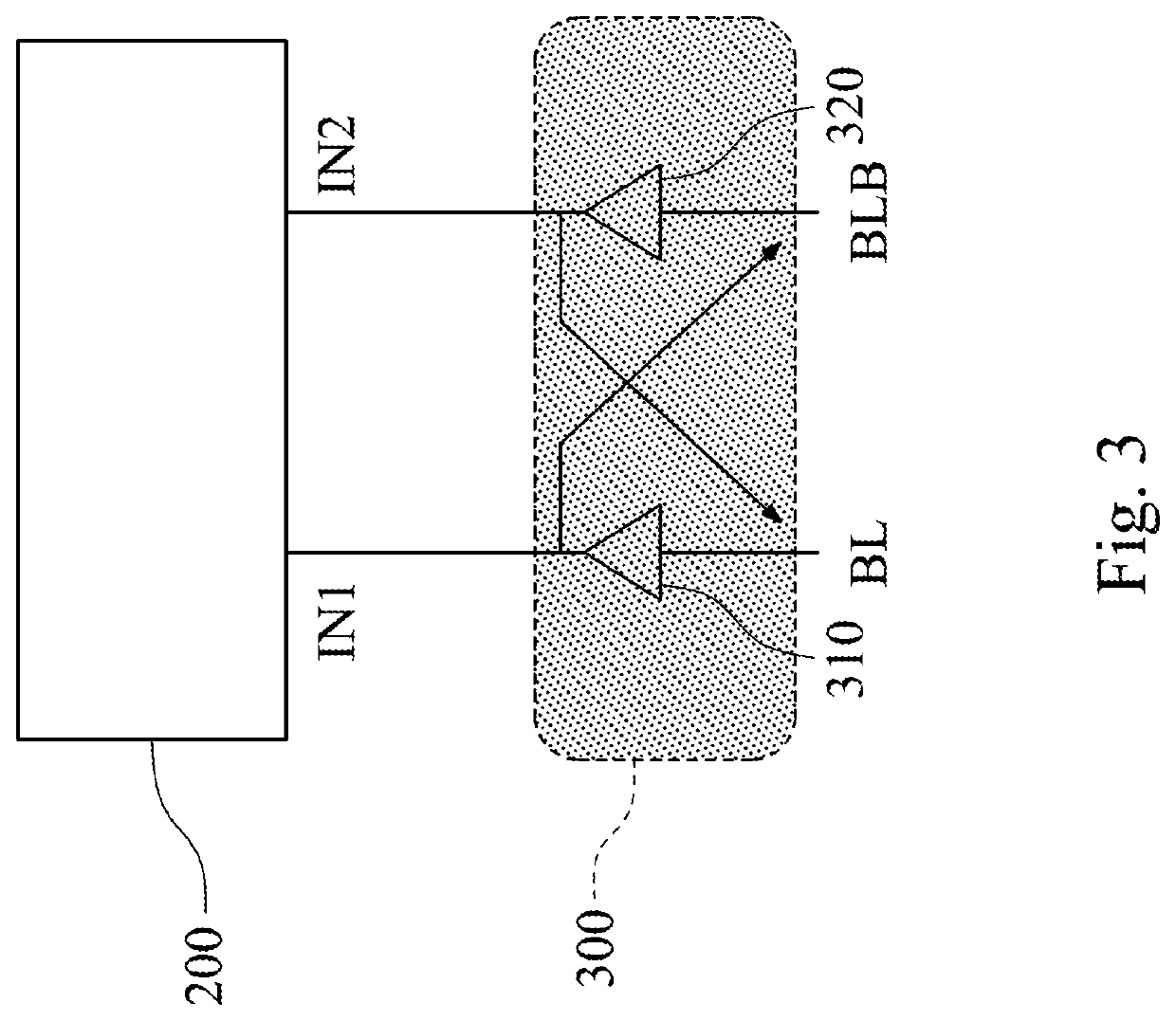
[0021]FIG. 1 shows a block diagram of a voltage-enhanced-feedback sense amplifier 100 of a resistive memory according to one embodiment of the present disclosure; FIG. 2 shows timing diagrams of voltages of a first bit line BL and a second bit line BLB of FIG. 1; FIG. 3 shows a schematic circuit diagram of the voltage-enhanced-feedback sense amplifier 100 of the resistive memory of FIG. 1; FIG. 4 shows a circuit diagram of a voltage sense amplifier 200 of the voltage-enhanced-feedback sense amplifier 100 of the resistive memory of FIG. 1; and FIG...


PUM


Abstract

A voltage-enhanced-feedback sense amplifier of a resistive memory is configured to sense a first bit line and a second bit line. The voltage-enhanced-feedback sense amplifier includes a voltage sense amplifier and a voltage-enhanced-feedback pre-amplifier. The voltage-enhanced-feedback pre-amplifier is electrically connected to the voltage sense amplifier. A first bit-line amplifying module receives a voltage level of the second input node to suppress a voltage drop of the first bit line and amplifies a voltage level of the first input node according to a voltage level of the first bit line. A second bit-line amplifying module receives the voltage level of the first input node to suppress a voltage drop of the second bit line and amplifies the voltage level of the second input node according to a voltage level of the second bit line. A margin enhanced voltage difference is greater than a read voltage difference.

Description

BACKGROUNDTechnical Field[0001]The present disclosure relates to a sense amplifier of a resistive memory and an operating method thereof. More particularly, the present disclosure relates to a voltage-enhanced-feedback sense amplifier of a resistive memory and an operating method thereof which are capable of enhancing effective sensing margin and increasing sensing yield.Description of Related Art[0002]In these years, due to the industrial growth of mobile device, medical electrical equipment, portable storage, etc., requirement of memory with low power, high speed and high density is increased. However, sensing margin time of the memory is the key factor which may limit the access time of the memory. It is known to provide memory circuitry including an array of bit cells within which columns of bit cells are connected by bit line pairs. The bit line pairs are precharged to a given voltage and then one of the bit lines of the pair is discharged depending upon the contents of the bit...

Claims


Application Information

Patent Timeline
Patent Type & Authority Applications(United States)
IPC IPC(8): G11C7/08G11C13/00G11C7/06G11C11/16G11C7/12
CPCG11C13/0026G11C7/08G11C11/1655G11C7/12G11C13/004G11C11/1673G11C2013/005G11C7/065G11C7/062G11C11/1693G11C13/0061G11C2013/0042
Inventor CHANG, MENG-FANLIN, HUAN-TING
Owner NATIONAL TSING HUA UNIVERSITY
Learn More