Memory device

Active Publication Date: 2020-04-02
WINBOND ELECTRONICS CORP
View PDF7 Cites 0 Cited by
  • Summary
  • Abstract
  • Description
  • Claims
  • Application Information

AI Technical Summary

Benefits of technology

[0005]The disclosure provides a memory device in which a data receiver and other peripheral circuits are driven by operating voltages

Problems solved by technology

Nevertheless, when the data receiver of the memory device is driven by a lower operating voltage, a decrease in speed of the memory device may occ

Method used


Image

  • Memory device
  • Memory device
  • Memory device

Examples


Embodiment Construction

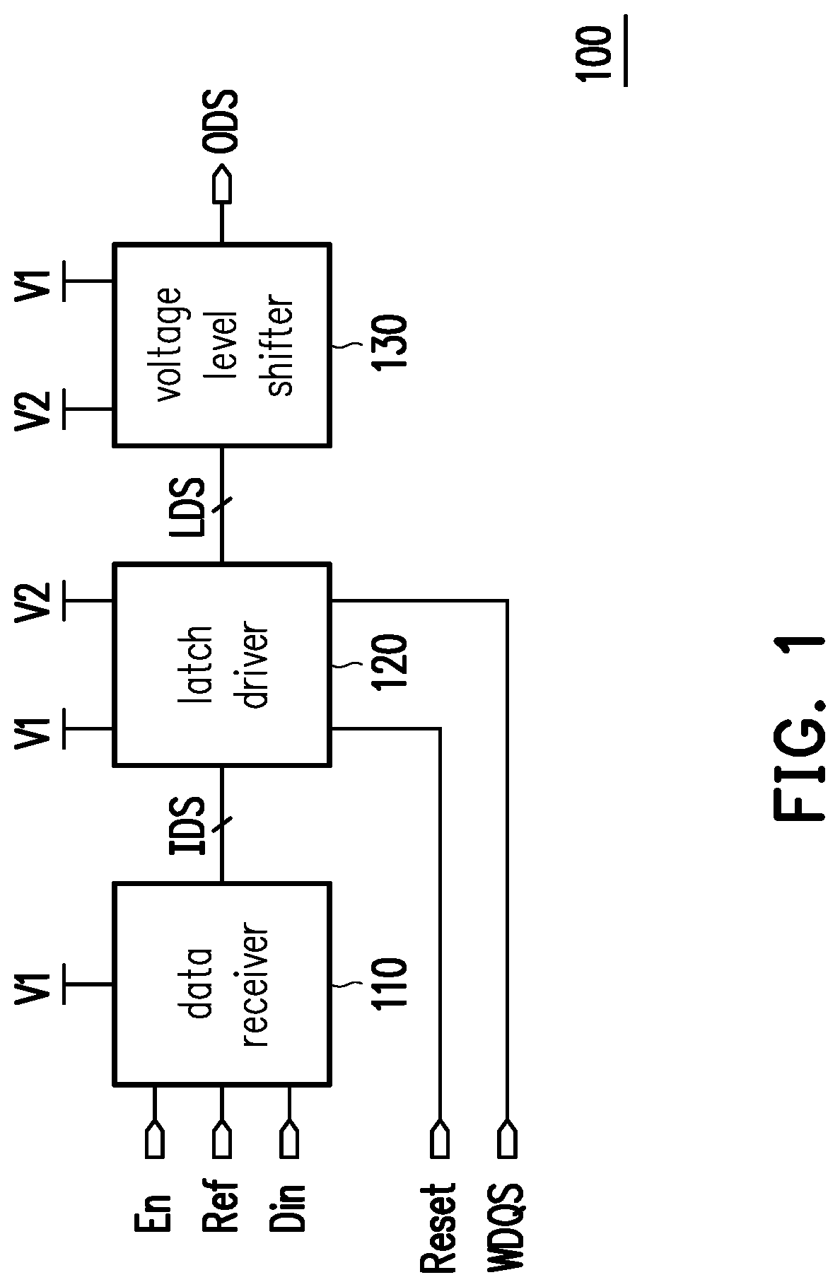
[0015]With reference to FIG. 1, FIG. 1 is a schematic diagram illustrating circuit blocks of a memory device according to an embodiment of the disclosure. A memory device 100 includes a data receiver 110, a latch driver 120, and a voltage level shifter 130. The data receiver 110 works in a first voltage V1, receives an enable signal En, a reference signal Ref, and an input data signal Din, and the data receiver 110 outputs an internal data signal IDS to the latch driver 120 by the first voltage V1. The latch driver 120 is coupled to the data receiver 110, works in the first voltage V1 and a second voltage V2, and receives a reset signal Reset, a write select signal WDQS, and the internal data signal IDS from the data receiver 110. Herein, the latch driver 120 may perform a reset operation by the reset signal Reset and may perform a writing operation by the write select signal WDQS.

[0016]Next, the latch driver 120 latches the internal data signal IDS by the first voltage V1 and outpu...


PUM


Abstract

A memory device includes a data receiver, a latch driver, and a voltage level shifter. The data receiver works in a first voltage, receives an enable signal, a reference signal, and an input data signal, and outputs an internal data signal by the first voltage. The latch driver receives a write select signal and the internal data signal, latches the internal data signal by the first voltage, and outputs at least one latch data signal by a second voltage. The voltage level shifter receives the at least one latch data signal by the second voltage and generates at least one output data signal by the at least one latch data signal. The voltage level shifter sets a voltage value of the at least one output data signal by the first voltage. The voltage value of the first voltage is greater than the voltage value of the second voltage.

Description

CROSS-REFERENCE TO RELATED APPLICATION[0001]This application claims the priority benefit of Japan application serial no. 2018-182335, filed on Sep. 27, 2018. The entirety of the above-mentioned patent application is hereby incorporated by reference herein and made a part of this specification.BACKGROUNDTechnical Field[0002]The disclosure relates to a memory device. More particularly, the disclosure relates to a memory device capable of increasing an operating speed and lowering power consumption.Description of Related Art[0003]In a conventional standard semiconductor memory device featuring the low power double data rate 4×(LPDDR4×), in order to lower power consumption, the data receiver in the memory device is designed to have a lower operating voltage (e.g., 0.6 volt), and peripheral circuits of the memory device are designed to have higher operating voltages (e.g., 1.1 volts).[0004]Nevertheless, when the data receiver of the memory device is driven by a lower operating voltage, a...

Claims


Application Information

Patent Timeline
IPC IPC(8): G11C7/10H03K19/0185
CPCH03K19/018507G11C7/1087H03F3/45179G11C7/1096G11C7/1084H03K3/356147H03F3/45183H03F2203/45506H03F2203/45674
Inventor NAKAOKA, YUJI
Owner WINBOND ELECTRONICS CORP
Why Eureka
Try Eureka