

Semiconductor device and dynamic logic circuit
- Summary
- Abstract
- Description
- Claims
- Application Information
AI Technical Summary
Benefits of technology
Problems solved by technology
Method used
Image

Examples
embodiment 1
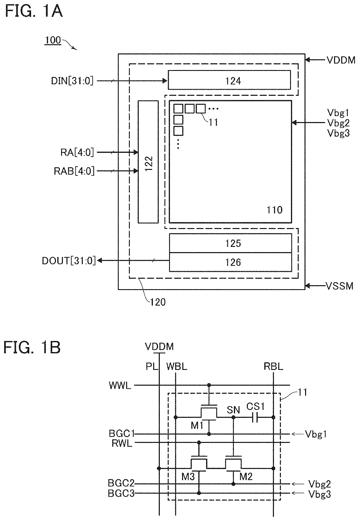
[0050]As an example of a semiconductor device, a memory device including OS transistors is described. A memory device 100 illustrated in FIG. 1A includes a memory cell array 110 and a peripheral circuit 120. Voltages VDDM, VSSM, Vbg1, Vbg2, and Vbg3 and other voltages are input to the memory device 100. The voltages VDDM and VSSM are respectively a high power supply voltage and a low power supply voltage. The voltage VSSM is a ground potential (GND), for example.
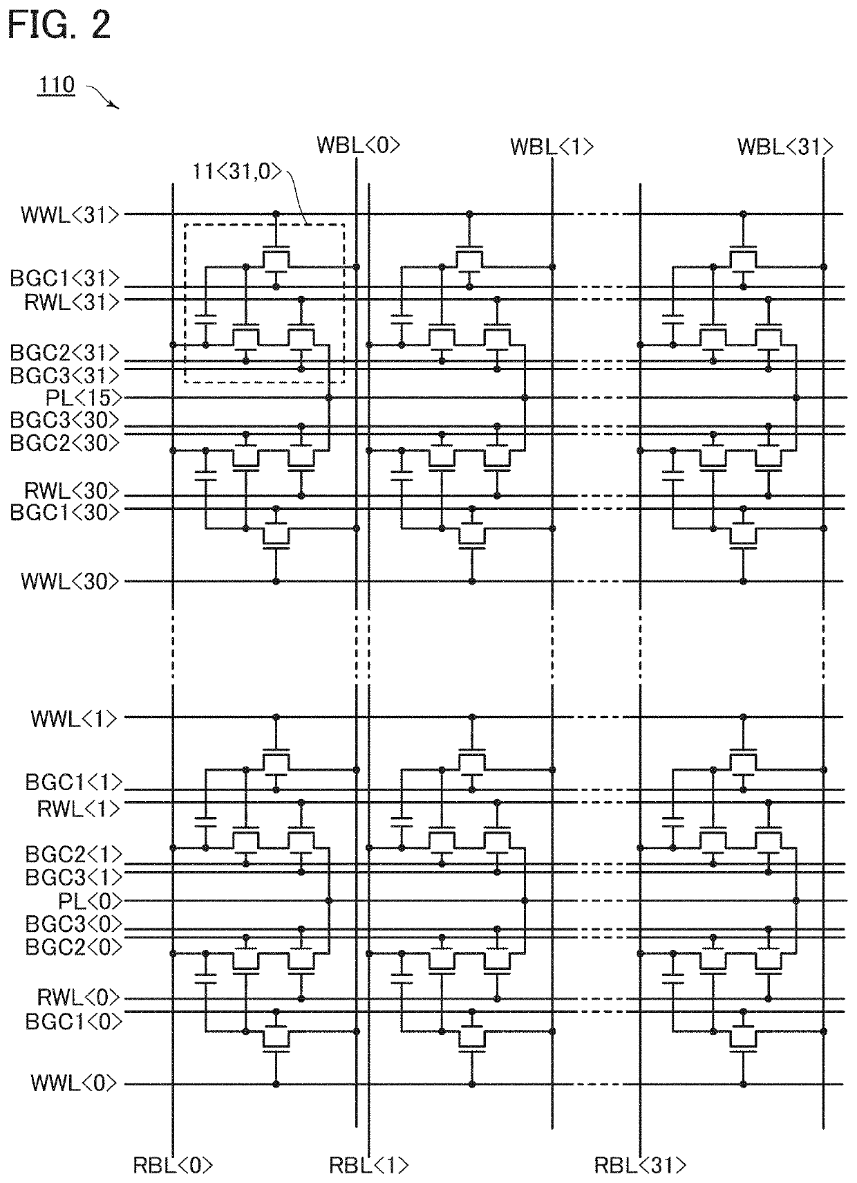
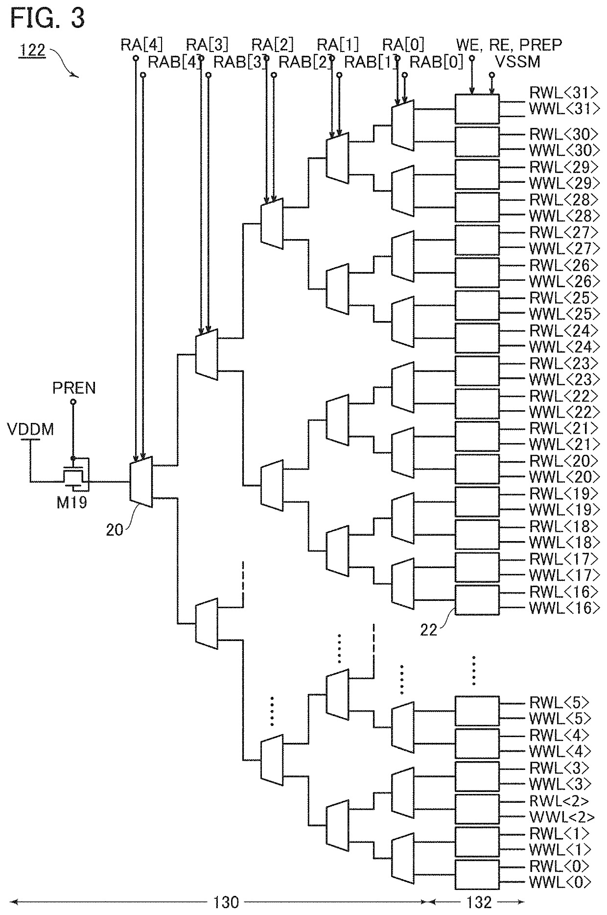
[0051]The memory cell array 110 and the peripheral circuit 120 include OS transistors. The memory cell array 110 includes a plurality of memory cells 11. In this example, the memory cells 11 are arranged in 32 rows and 32 columns. The peripheral circuit 120 includes a row decoder 122, a write circuit 124, a read circuit 125, and an output circuit 126. Data DIN[31:0], address signals RA[4:0], address signals RAB[4:0], and various control signals are input to the peripheral circuit 120. In this example, the memory width of the...
embodiment 2
[0133]A manufacturing technique for OS transistors is compatible with a CMOS manufacturing technique, and a single-conductivity-type memory device including OS transistors can be stacked over a CMOS logic circuit. In this embodiment, a semiconductor device that includes a CMOS circuit using Si transistors and a single-conductivity-type circuit using OS transistors is described.
[0134]When including only OS transistors, the memory device in Embodiment 1 is suitable for a relatively small-scale (e.g., 128-bit to 1-Mbit) memory device.
[0135]For example, an embedded memory device 205 of an application processor (AP) 200 illustrated in FIG. 11 includes the memory device described in Embodiment 1. FIG. 11 is a schematic view of a chip of the AP 200. The AP 200 is a system-on-chip. The chip of the AP 200 has a stacked-layer structure including a CMOS transistor layer 221 and an OS transistor layer 222. The CMOS transistor layer 221 is provided with various kinds of functional circuits inclu...
embodiment 3
[0151]Structure examples of OS transistors will be described with reference to FIGS. 14A and 14B. Cross-sectional views of the OS transistors in the channel length direction are shown on the left side of FIGS. 14A and 14B, and cross-sectional views of the OS transistors in the channel width direction are shown on the right side of FIGS. 14A and 14B.
[0152]An OS transistor 5001 illustrated in FIG. 14A is formed over an insulating surface, here, over an insulating layer 5021. The OS transistor 5001 is covered with insulating layers 5028 and 5029. The OS transistor 5001 includes insulating layers 5022, 5023, 5024, 5025, 5026, 5027, 5028, 5029, 5030, and 5031, metal oxide layers 5011, 5012, and 5013, and conductive layers 5050, 5051, 5052, 5053, and 5054.
[0153]Note that an insulating layer, a metal oxide layer, a conductive layer, and the like in a drawing may have a single-layer structure or a layered structure. These components can be formed by any of a variety of deposition methods su...
PUM
 Abstract
Description
Claims
Application Information