

Semiconductor device
- Summary
- Abstract
- Description
- Claims
- Application Information
AI Technical Summary
Benefits of technology
Problems solved by technology
Method used
Image

Examples
first embodiment
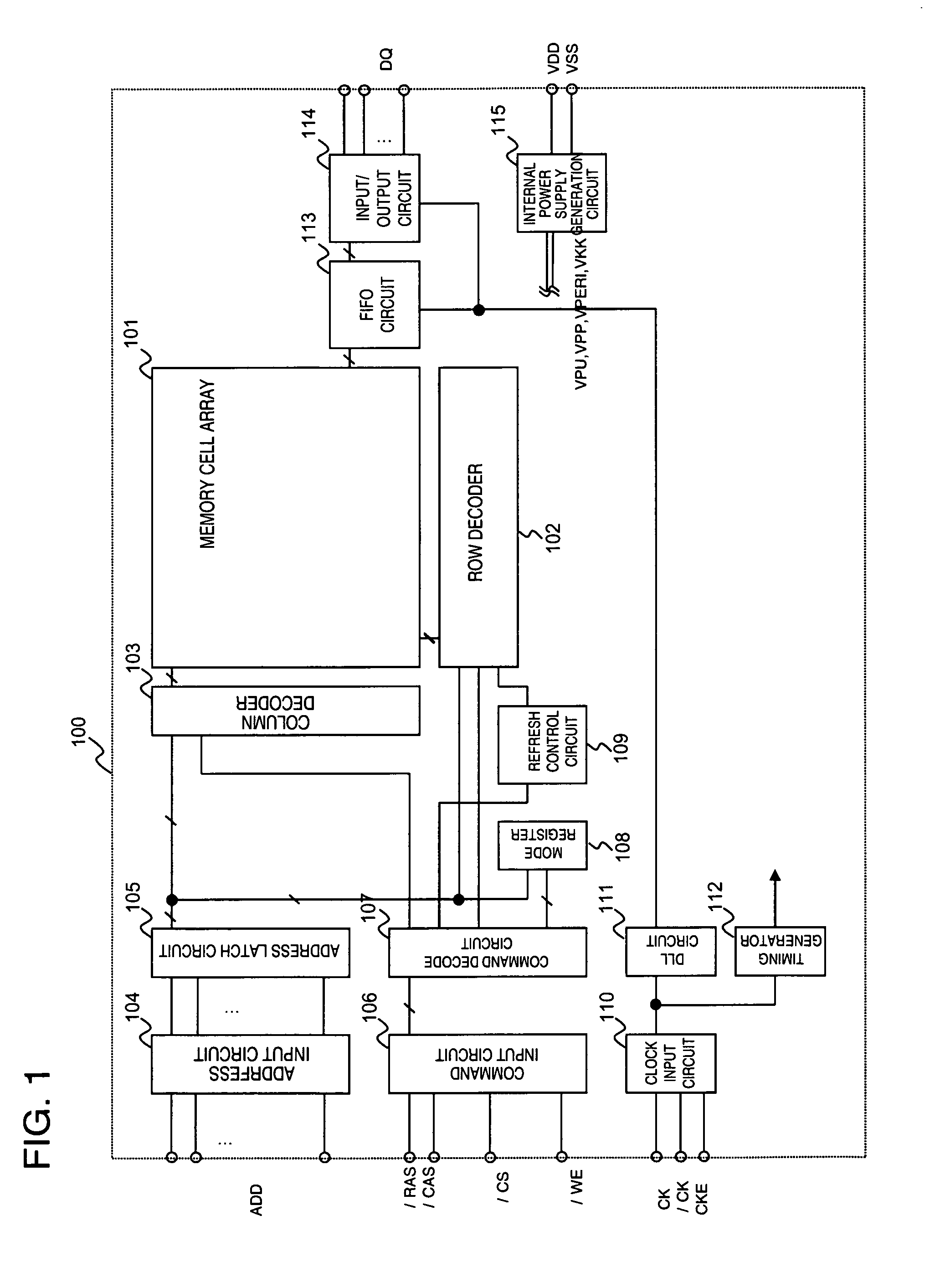
[0062]An internal power supply generation circuit 115 generates internal power supplies (a voltage VPU and a boosted voltage VPP, which will be described later). The voltage VPU and the voltage VPP are high voltages, a voltage VPERI is an internal operation voltage, a voltage VKK is a negative voltage lower than a GND potential (0V). A potential of a non-selected word line is set to the negative voltage VKK. Referring to FIG. 1, the internal power supply generation circuit 115 outputs the voltage VPU. In a first embodiment that will be described below, however, a level of the voltage VPU is generated by a generation circuit of an FX signal that provides a high potential of a word line. Thus, it is not necessary to generate the power supply voltage VPU at the internal power supply generation circuit 115. Potential levels of these voltages are in a relationship of VPU>VPP>VDD>VPERI>VSS (=0V)>VKK.
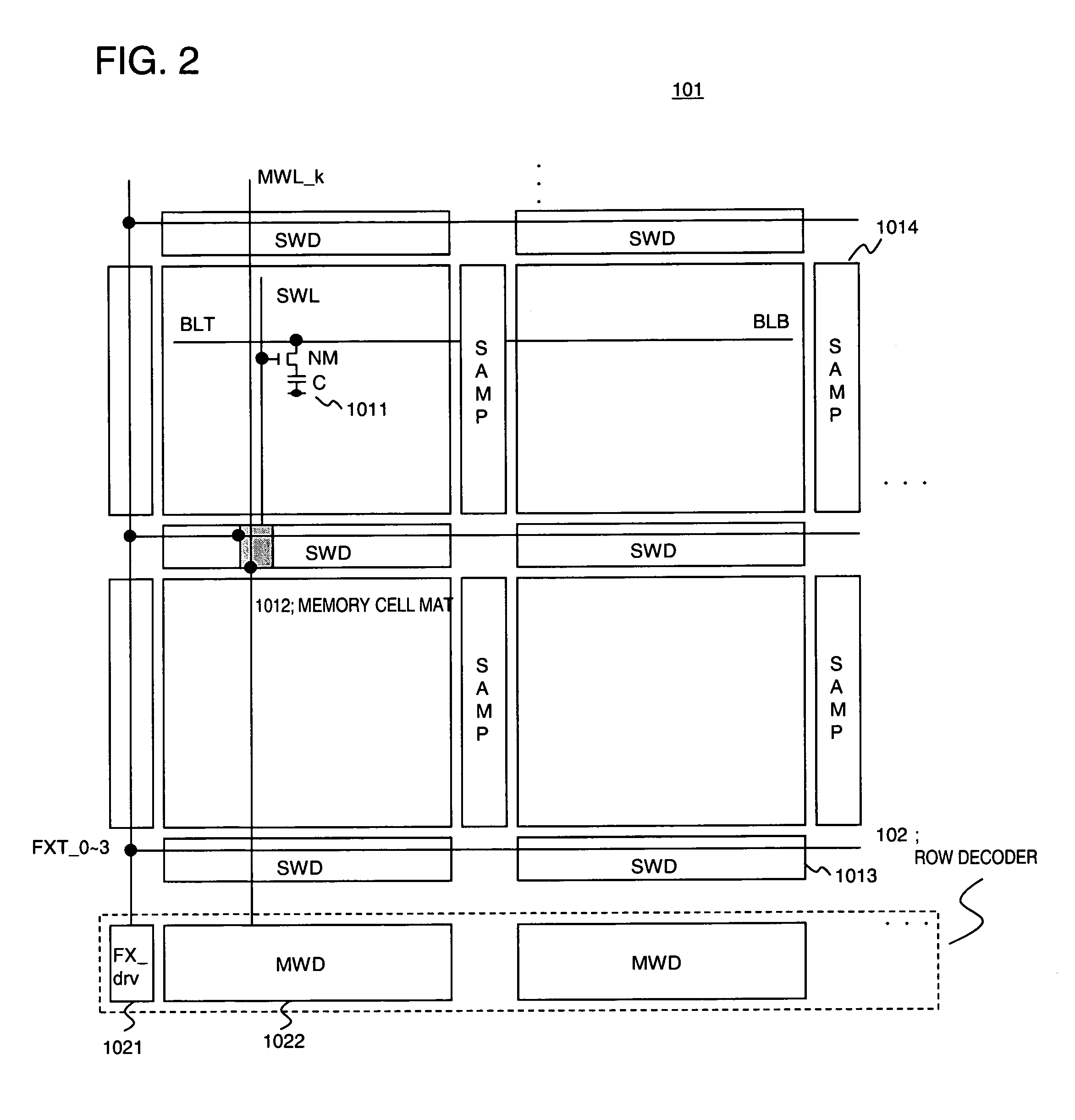
[0063]Reference symbols FXT / FXB, and (Main Word Line: main word line) that will be describ...
second embodiment
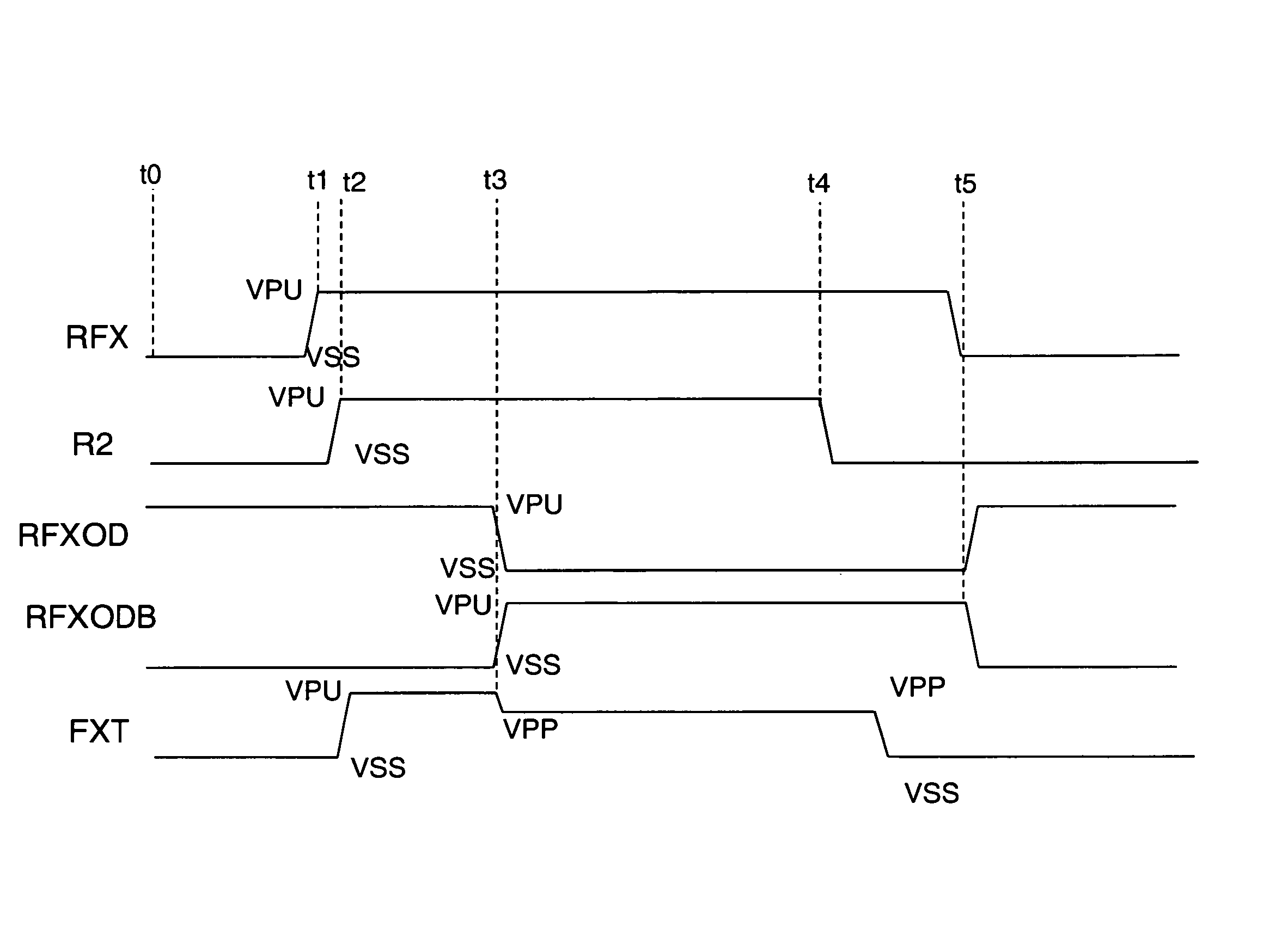
[0101]FIG. 7 is a signal waveform diagram illustrating an example of operation in the FIG. 7 shows signal waveforms of signals RFX, R2, RFXOD, RFXODB, and FXT in FIG. 6. The signals RFX and FXT respectively correspond to a selected one of signals RFX_i and a selected one of signals FXT_i (i=0 to 3). In the following description, a suffix (_i) in each of the signals RFX_i and FXT_i will be omitted. Timings t0 to t5 correspond to the timings t0 to t5 in FIG. 5. An ACT command, a READ command, and a PRE command are respectively received at the timings t0, t4, and t5.
[0102]At the timing t0, the signal RFX is Low (VSS), the signal R2 is Low, the signal RFXOD is High (VPU), and the signal RFXODB is Low. The output node N21 of the NAND circuit NAND is High. The NMOS transistor NM21 turns on and the PMOS transistors PM23 and PM24 turn off. The CMOS transfer gate (PM22, NM22) turns on, a High potential at the node N21 is transmitted to the node N22, the PMOS transistor PM25 turns off, and t...
third embodiment
[0117]FIG. 9 is a waveform diagram illustrating the operation of a Timings t0, t1, t2, and t3 correspond respectively to the timings to, t1, t3, and t5 in FIG. 4. Reference symbol RFX indicates a selected one of the signals RFX_0 to RFX_3 in FIG. 8, and a suffix added to the signal RFX_i will be omitted in the following description.
[0118]At the timing t0, the signal RFX is Low, the signal RFXOD is High (VPU), and a power supply voltage VFX is High (VPU), and the output node N31 of the NAND circuit NAND is High (VPU). Thus, the PMOS transistor PM33 is off. Since the signal RFX is Low (VSS), the PMOS transistor PM31 turns on and the node N32 is High (VPU). The NMOS transistor NM32 turns on, and a voltage of the signal FXT is set to a voltage VSS (VSS).
[0119]At the timing t1, the signal RFX rises to High (VPU), the PMOS transistor PM31 turns off and the NMOS transistor NM31 turns on. The node N32 goes Low (VSS), the PMOS transistor PM32 turns on and the NMOS transistor NM32 turns off....
PUM
 Abstract
Description
Claims
Application Information