Semiconductor device and fabrication method thereof

Active Publication Date: 2020-05-07
SEMICON MFG INT (SHANGHAI) CORP +1
View PDF0 Cites 2 Cited by
  • Summary
  • Abstract
  • Description
  • Claims
  • Application Information

AI Technical Summary

Benefits of technology

[0007]Another aspect of the present disclosure includes a semiconductor device. The semiconductor device includes a semiconductor substrate having a middle region and an edge region adjacent to the middle region. A surface of the middle region of the semiconductor substrate is higher than a surface of the edge region of the semiconductor substrate. The semiconductor device may also include a plurality of first fins formed

Problems solved by technology

A conventional planar device usually has a weak control on its channel current, and a short channel effect is easy to oc

Method used


Image

  • Semiconductor device and fabrication method thereof
  • Semiconductor device and fabrication method thereof
  • Semiconductor device and fabrication method thereof

Examples


Embodiment Construction

[0013]Reference will now be made in detail to exemplary embodiments of the disclosure, which are illustrated in the accompanying drawings. Wherever possible, the same reference numbers will be used throughout the drawings to refer to the same or like parts.

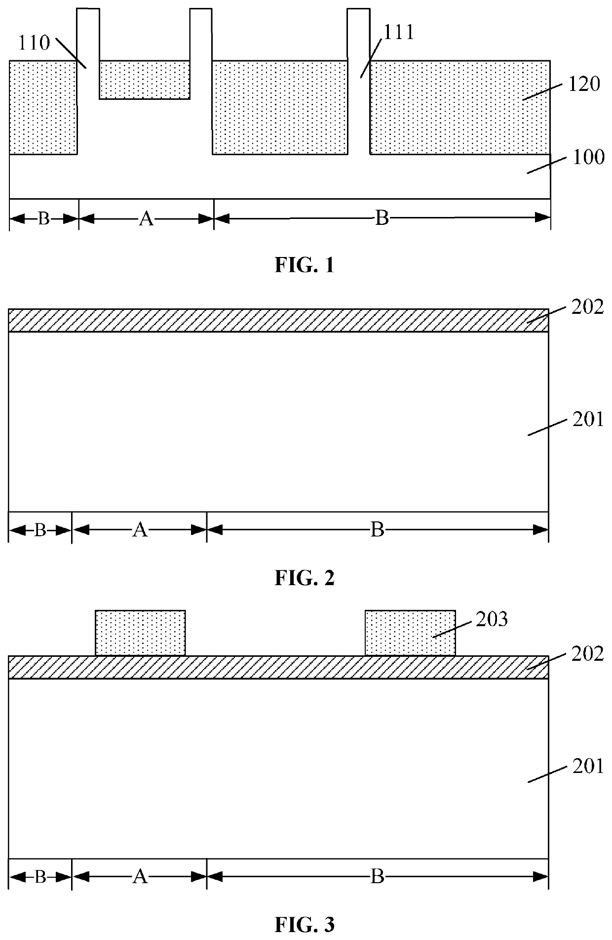
[0014]FIG. 1 illustrates a semiconductor device. As shown in FIG. 1, the semiconductor device includes a semiconductor substrate 100. The semiconductor substrate 100 includes a middle region A and an edge region B adjacent to the middle region A. The surface of the middle region A is higher than the edge region B of the surface of the semiconductor substrate 100. Further, the semiconductor device includes a plurality of discrete first fins 110 on the surface of the middle region A of the semiconductor substrate 100; and a plurality of discrete second fins 111 on the surface of the edge region B of the semiconductor substrate 100. Further, the semiconductor device includes an isolation structure 120 on the surface of the semiconduc...


PUM


Abstract

Semiconductor devices and fabrication methods are provided. An exemplary fabrication method includes providing an initial base substrate having a middle region and an adjacent edge region; forming a first opening in the middle region of the initial base substrate; forming a first adjustment layer on sidewall surfaces of the first opening; and forming a plurality of second openings with a depth greater than a depth of the first opening in the edge region of the initial base substrate. A portion of the initial base substrate between the first opening and the second opening forms a first fin, a portion of the initial base substrate between adjacent second openings form a second fin. The method also includes forming an isolation structure with a top surface lower than top surfaces of the first fin and the second fins on the surface of the initial base substrate.

Description

CROSS-REFERENCES TO RELATED APPLICATIONS[0001]This application claims the priority of Chinese patent application No. 201811295011.1, filed on Nov. 1, 2018, the entirety of which is incorporated herein by reference.FIELD OF THE DISCLOSURE[0002]The present disclosure generally relates to the field of semiconductor manufacturing and, more particularly, relates to semiconductor devices and fabrication methods.BACKGROUND[0003]With the rapid development of the semiconductor manufacturing technologies, integrated circuits (ICs) are being developed toward higher component densities and higher integration level. As one of the basic components of ICs, semiconductor devices are widely used. A conventional planar device usually has a weak control on its channel current, and a short channel effect is easy to occur to have a leakage current issue. Thus, the electrical performance of the semiconductor devices is adversely affected.[0004]To overcome the short channel effect of the semiconductor dev...

Claims


Application Information

Patent Timeline
IPC IPC(8): H01L29/78H01L29/06H01L21/02H01L21/306H01L21/308H01L21/762H01L29/66
CPCH01L21/0217H01L29/7846H01L21/30604H01L29/66795H01L29/0653H01L29/7851H01L21/76229H01L21/02164H01L21/3086H01L29/7855H01L29/7843H01L29/84H01L21/31116H01L21/31138H01L21/823431H01L27/0886H01L21/3083H01L21/31122
Inventor ZHOU, FEI
Owner SEMICON MFG INT (SHANGHAI) CORP
Why Eureka
Try Eureka