Display Device

a technology for displaying devices and bezels, applied in static indicating devices, instruments, other domestic objects, etc., can solve problems such as reducing display area, and achieve the effect of reducing bezel area

Active Publication Date: 2020-05-28
LG DISPLAY CO LTD
View PDF0 Cites 17 Cited by
  • Summary
  • Abstract
  • Description
  • Claims
  • Application Information

AI Technical Summary

Benefits of technology

[0009]To achieve these objects and other advantages and in accordance with the purpose of the disclosure, as embodied and broadly described herein, a display device includes a substrate including at least one hole area disposed within an emission area, and at least one blocking hole passing through inorganic insulating films disposed beneath a light emitting element while including upper and lower

Problems solved by technology

For this reason, conventional display devices h

Method used


Image

  • Display Device
  • Display Device
  • Display Device

Examples


first embodiment

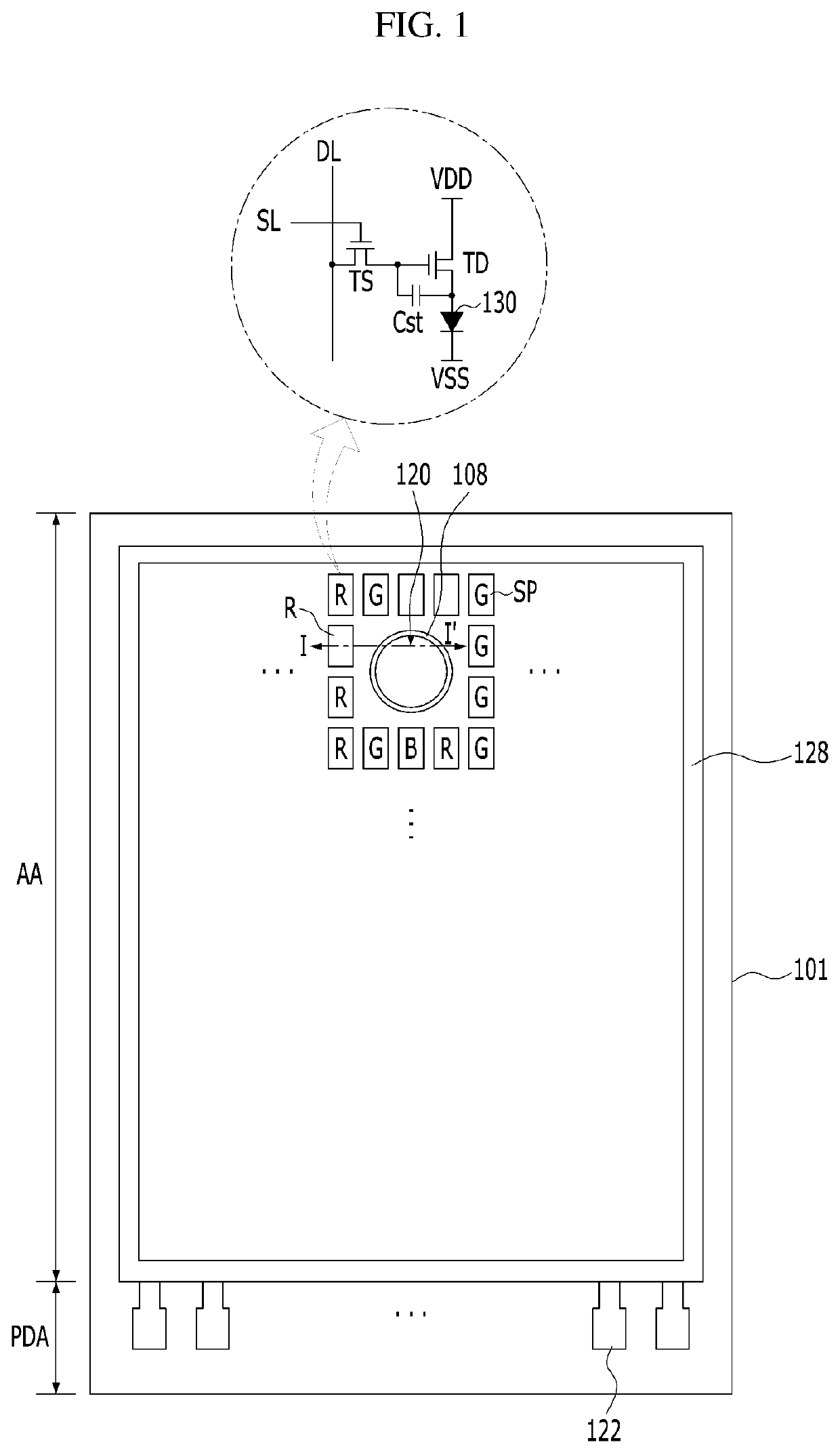
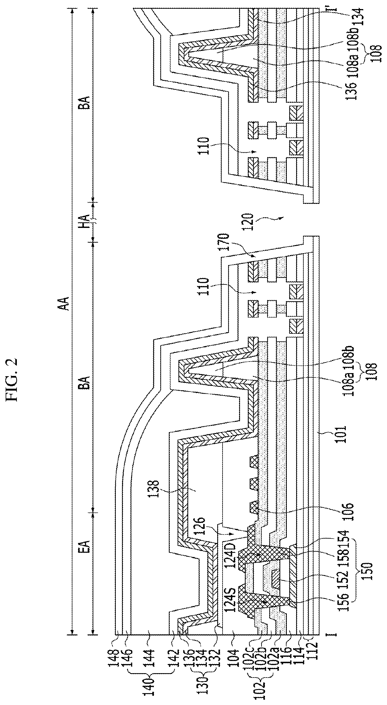
[0030]FIG. 2 illustrates a display device according to the present disclosure. As illustrated in FIG. 2, the driving transistor TD, which is designated by reference numeral “150”, includes an active layer 154 disposed on an active buffer layer 114, a gate electrode 152 overlapping with the active layer 154 under the condition that a gate insulating film 116 is interposed between the active layer 154 and the gate electrode 152, and a source electrode 156 and a drain electrode 158 formed on an interlayer insulating film 102 while contacting the active layer 154.

[0031]The active layer 154 is made of at least one of an amorphous semiconductor material, a polycrystalline semiconductor material, or an oxide semiconductor material. The active layer 154 includes a channel region, a source region, and a drain region. The channel region overlaps with the gate electrode 152 under the condition that the gate insulating film 116 is interposed between the channel region and the gate electrode 152...

second embodiment

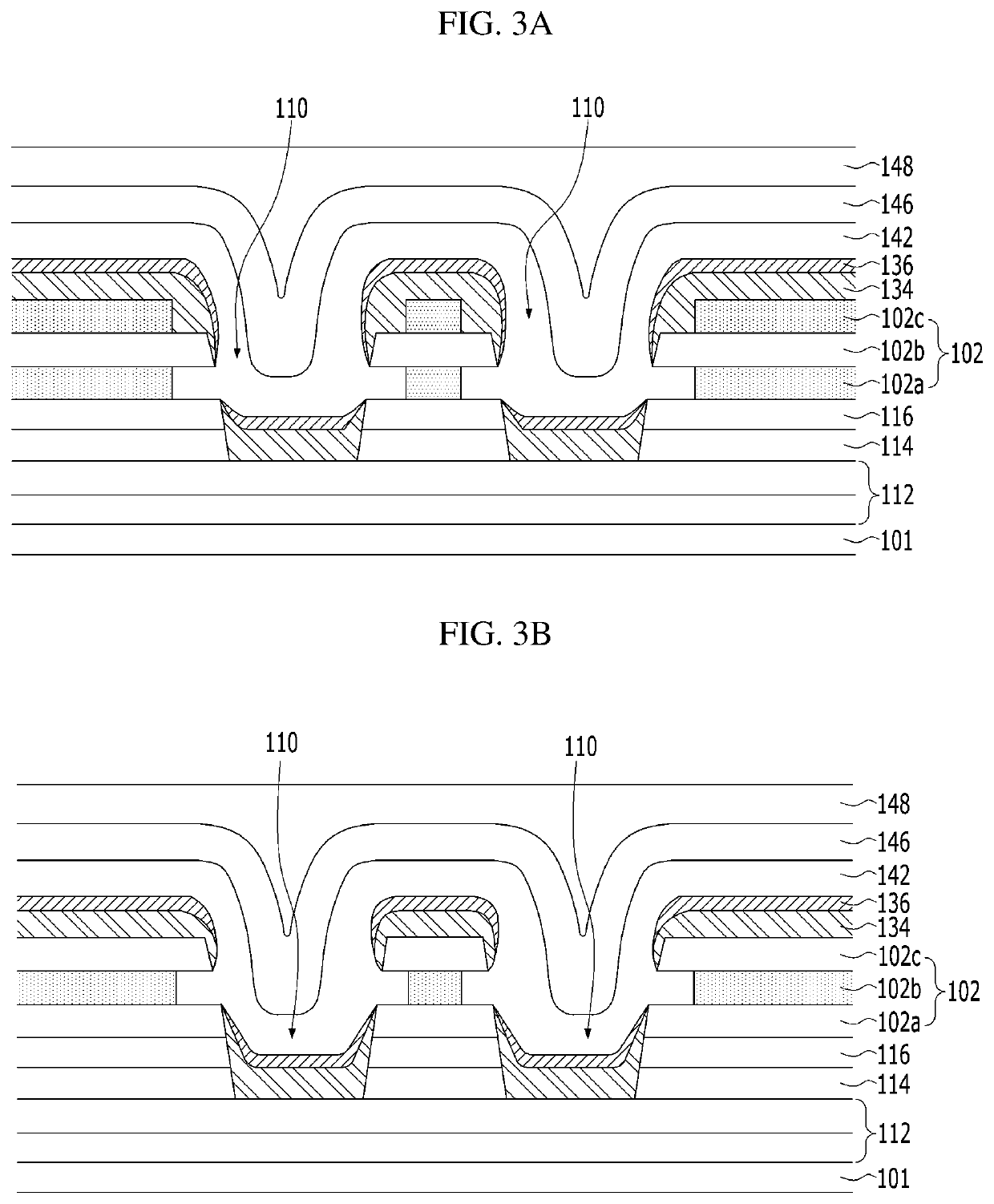
[0070]FIG. 6 is a cross-sectional view illustrating a display device according to the present disclosure.

[0071]The display device illustrated in FIG. 6 includes the same constituent elements as those of the display device illustrated in FIG. 2, except that a hard mask pattern 180 is further included. Accordingly, no detailed description will be given of the same constituent elements for the sake of brevity.

[0072]The hard mask pattern 180 is formed on the uppermost interlayer insulating film 102c of the interlayer insulating film 102 having a multilayer structure, using one of ITO, MoTi, Mo, and Ti, to have a single-layer structure or a multilayer structure. Although the hard mask pattern 180 is removed in the above-described process of FIGS. 5A-5C, the hard mask pattern 180 is left on the substrate 101 without being removed in this case. For example, a photoresist pattern having a multi-step structure may be formed through a photolithography process using a half-tone mask, and the h...

third embodiment

[0076]FIG. 8 is a cross-sectional view illustrating a display device according to the present disclosure.

[0077]The display device illustrated in FIG. 8 includes the same constituent elements as those of the display device illustrated in FIG. 2, except that a passivation film 118 is further included. Accordingly, no detailed description will be given of the same constituent elements for the sake of brevity.

[0078]The passivation film 118 is formed between the thin film transistor (TD) 150 and the anode 132. That is, the passivation film 118 is disposed on the uppermost interlayer insulating film 102c of the interlayer insulating film 102 having a multilayer structure. The passivation film 118 is made of a material different from that of the third interlayer insulating film 102c, which is the uppermost interlayer insulating film. For example, the passivation film 118 and the second interlayer insulating film 102b are made of SiOx, whereas the first and third interlayer insulating films...


PUM


Abstract

A display device capable of reducing a non-display area includes a substrate including at least one hole area disposed within an emission area, and at least one blocking hole passing through inorganic insulating films disposed beneath a light emitting element while including upper and lower insulating films made of different materials. Side surfaces of the upper inorganic insulating film exposed through the blocking hole protrude beyond side surfaces of the lower inorganic insulating film exposed through the blocking hole, respectively. Accordingly, it is possible to minimize a bezel area, which is a non-display area, and to disconnect a light emitting stack by the blocking hole.

Description

CROSS-REFERENCE TO RELATED APPLICATIONS[0001]This application claims the benefit of Republic of Korea Patent Application No. 10-2018-0145431 filed on Nov. 22, 2018, which is hereby incorporated by reference as if fully set forth herein.BACKGROUNDField[0002]The present disclosure relates to a display device, and more particularly to a display device capable of reducing a non-display area.Discussion of the Related Art[0003]An image display device, which renders a variety of information on a screen, is a core technology of the information age. Such an image display device is developing towards enhanced thinness, enhanced lightness, and enhanced portability as well as enhanced performance. In connection with this, a flat display device capable of eliminating disadvantages of heavy and bulky structures of cathode ray tubes (CRTs) is highlighted.[0004]Representative examples of such a flat display device may include a liquid crystal display (LCD) device, a plasma display panel (PDP), an o...

Claims


Application Information

Patent Timeline
IPC IPC(8): H01L27/32H01L51/00H01L51/52
CPCH01L27/3258H01L51/5253H01L51/0096H10K59/12Y02E10/549H10K50/844H10K59/351H10K59/00H10K50/80H10K50/84G09G2300/0465B32B2457/206H10K59/124H10K77/10
Inventor SON, SEOK-WOOYUN, JEONG-GIPARK, JONG-HANKIM, JO-YEON
Owner LG DISPLAY CO LTD
Why Eureka
Try Eureka