Split Gate Non-volatile Memory Cells With FINFET Structure And HKMG Memory And Logic Gates, And Method Of Making Same

a non-volatile memory, logic gate technology, applied in the direction of semiconductor devices, electrical devices, transistors, etc., can solve the problem of adding to the cost of making the devi

Active Publication Date: 2020-06-04
SILICON STORAGE TECHNOLOGY
View PDF5 Cites 9 Cited by
  • Summary
  • Abstract
  • Description
  • Claims
  • Application Information

AI Technical Summary

Benefits of technology

[0005]The aforementioned problems and needs are addressed by a memory device that includes a semiconductor substrate having an upper surface with a plurality of upwardly extending fins, wherein each of the fins includes first and second side surfaces that oppose each other and that terminate in a top surface, a memory cell formed on a first fin of the plurality of fins and a logic device formed on a second fin of the plurality of fins. The memory cell includes spaced apart first source and first drain regions in the first fin, with a first channel region of the first fin extending along the top surface and the opposing side surfaces of the first fin between the first source and first drain regions, a floating gate of polysilicon material that extends along a first portion of the first channel region, wherein the floating gate extends along and is insulated from the first and second side surfaces and the top surface of the first fin, a select gate of metal material that extends along a second portion of the first channel region, wherein the select gate extends along and is insulated from the first and second side surfaces and the top surface of the first fin, a control gate of polysilicon material that extends along and is insulated from the floating gate, and an erase gate of polysilicon material that extends along and is insulated from the first source region. The logic device includes spaced apart second source and second drain regions in the second fin, with a second channel region of the second fin extending along the top surface and the opposing side surfaces of the second fin between the second source and second drain regions, and a first logic gate of metal material that extends along the second channel region, wherein the first logic gate extends along and is insulated from the first and second side surfaces and the top surface of the second fin.

Problems solved by technology

However, these prior art Fin-FET structures have disclosed using the floating gate in stacked gate configuration, or using trapping material, or using SRO (silicon rich oxide) or using nanocrystal silicon to store charges, or other more complicated memory cell configurations which can add to the cost of making the device.

Method used


Image

  • Split Gate Non-volatile Memory Cells With FINFET Structure And HKMG Memory And Logic Gates, And Method Of Making Same
  • Split Gate Non-volatile Memory Cells With FINFET Structure And HKMG Memory And Logic Gates, And Method Of Making Same
  • Split Gate Non-volatile Memory Cells With FINFET Structure And HKMG Memory And Logic Gates, And Method Of Making Same

Examples


Embodiment Construction

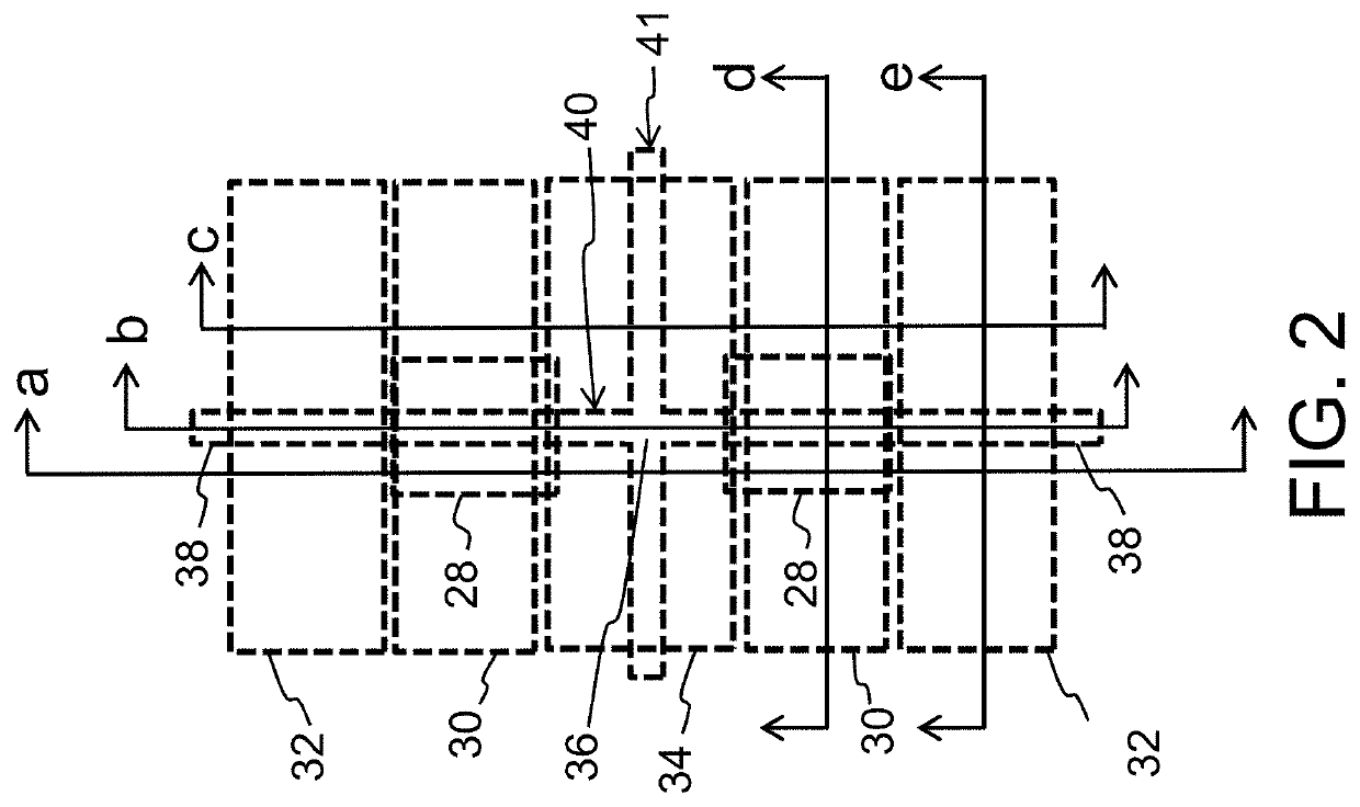
[0015]The present embodiments enable a memory device having Fin-FET split gate type memory cells each having four gates: a floating gate 28, control gate 30, a select gate 32 and an erase gate 34. Fin-FET logic devices are formed on the same substrate as the memory cells. FIG. 2 is a top view illustrating the configuration of a mirror pair of memory cells in the memory area of the substrate. The mirror pair of memory cells share a common source region 36 (i.e., a region of the substrate having a second conductivity type different than the first conductivity type of the substrate), where drain regions 38 (of the second conductivity type) are shared among adjacent pairs of memory cells (not shown). The substrate includes crossing fin shaped portions 40 and 41 of the upper surface of a semiconductor substrate 42. The memory cells are formed on the fin shaped portions 40. FIG. 2 further shows the cross sectional view directions a, b, c, d and e for subsequently described figures.

[0016]T...


PUM


Abstract

A memory device having plurality of upwardly extending semiconductor substrate fins, a memory cell formed on a first fin and a logic device formed on a second fin. The memory cell includes source and drain regions in the first fin with a channel region therebetween, a polysilicon floating gate extending along a first portion of the channel region including the side and top surfaces of the first fin, a metal select gate extending along a second portion of the channel region including the side and top surfaces of the first fin, a polysilicon control gate extending along the floating gate, and a polysilicon erase gate extending along the source region. The logic device includes source and drain regions in the second fin with a second channel region therebetween, and a metal logic gate extending along the second channel region including the side and top surfaces of the second fin.

Description

FIELD OF THE INVENTION[0001]The present invention relates to non-volatile flash memory cell arrays.BACKGROUND OF THE INVENTION[0002]Split gate non-volatile memory devices are well known in the art. For example, U.S. Pat. No. 7,927,994 discloses a split gate non-volatile memory cell. FIG. 1 illustrates an example of such a split gate memory cell formed on a semiconductor substrate 12. Source and drain regions 16 and 14 are formed as diffusion regions in substrate 12, and define a channel region 18 there between. The memory cell includes four conductive gates: a floating gate 22 disposed over and insulated from a first portion of the channel region 18 and a portion of the source region 16, a control gate 26 disposed over and insulated from the floating gate 22, an erase gate 24 disposed over and insulated from the source region 16, and a select gate 20 disposed over and insulated from a second portion of the channel region 18. A conductive contact 10 can be formed to electrically conn...

Claims


Application Information

Patent Timeline
Patent Type & Authority Applications(United States)
IPC IPC(8): H01L27/11521H01L27/11526H01L27/11531H01L29/10H01L29/423H01L29/78H01L29/788H01L21/28H01L29/66
CPCH01L27/11531H01L29/66795H01L29/7851H01L29/1083H01L27/11526H01L27/11521H01L29/7883H01L29/66537H01L29/66825H01L29/42328H01L29/40114H10B41/41H10B41/49H01L29/788H10B41/30H10B41/40H10B41/42
Inventor ZHOU, FENGKIM, JINHOLIU, XIANJOURBA, SERGUEIDECOBERT, CATHERINEDO, NHAN
Owner SILICON STORAGE TECHNOLOGY
Why Eureka
Try Eureka