
Interconnect with Self-Forming Wrap-All-Around Barrier Layer

a technology of graphene barrier layer and interconnect, which is applied in the direction of electrical apparatus, semiconductor device details, semiconductor/solid-state device devices, etc., can solve the problems of increasing the resistance of cu-based interconnect, increasing the amount of cu, and increasing the resistan

Active Publication Date: 2020-07-30
IBM CORP
View PDF0 Cites 2 Cited by
  • Summary
  • Abstract
  • Description
  • Claims
  • Application Information

AI Technical Summary

Benefits of technology

The present invention provides a method of forming interconnects with a self-forming wrap-all-around graphene barrier layer. This allows for better protection and insulation of the interconnects, improving their performance and reliability. The method involves patterning a trench in a dielectric, embedding an interconnect in the trench, and depositing a graphene layer or a metal liner to form the wrap-all-around graphene barrier layer surrounding the interconnect. This results in an interconnect structure with improved electrical performance, resilience to strain, and reduced thermal conductivity.

Problems solved by technology

However, as device dimensions shrink, the resistance of Cu-based interconnects becomes very high.
Use of conventional barrier materials like titanium nitride (TiN), tantalum nitride (TaN), however, unduly limits the amount of Cu in the interconnect, thereby further increasing the resistance.
However, metals like Co can still diffuse into the surrounding dielectric.
Thus, a barrier is needed for reliability time-dependent dielectric breakdown (TDDB) and this barrier needs to be very thin to achieve low line resistance.

Method used


Image

  • Interconnect with Self-Forming Wrap-All-Around Barrier Layer
  • Interconnect with Self-Forming Wrap-All-Around Barrier Layer
  • Interconnect with Self-Forming Wrap-All-Around Barrier Layer

Examples

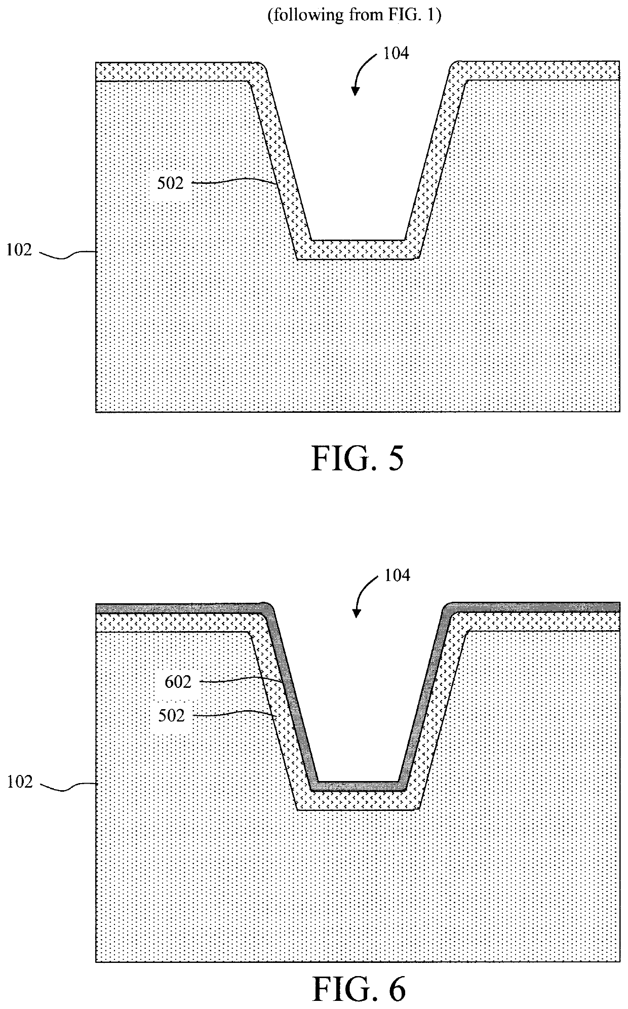

Embodiment Construction

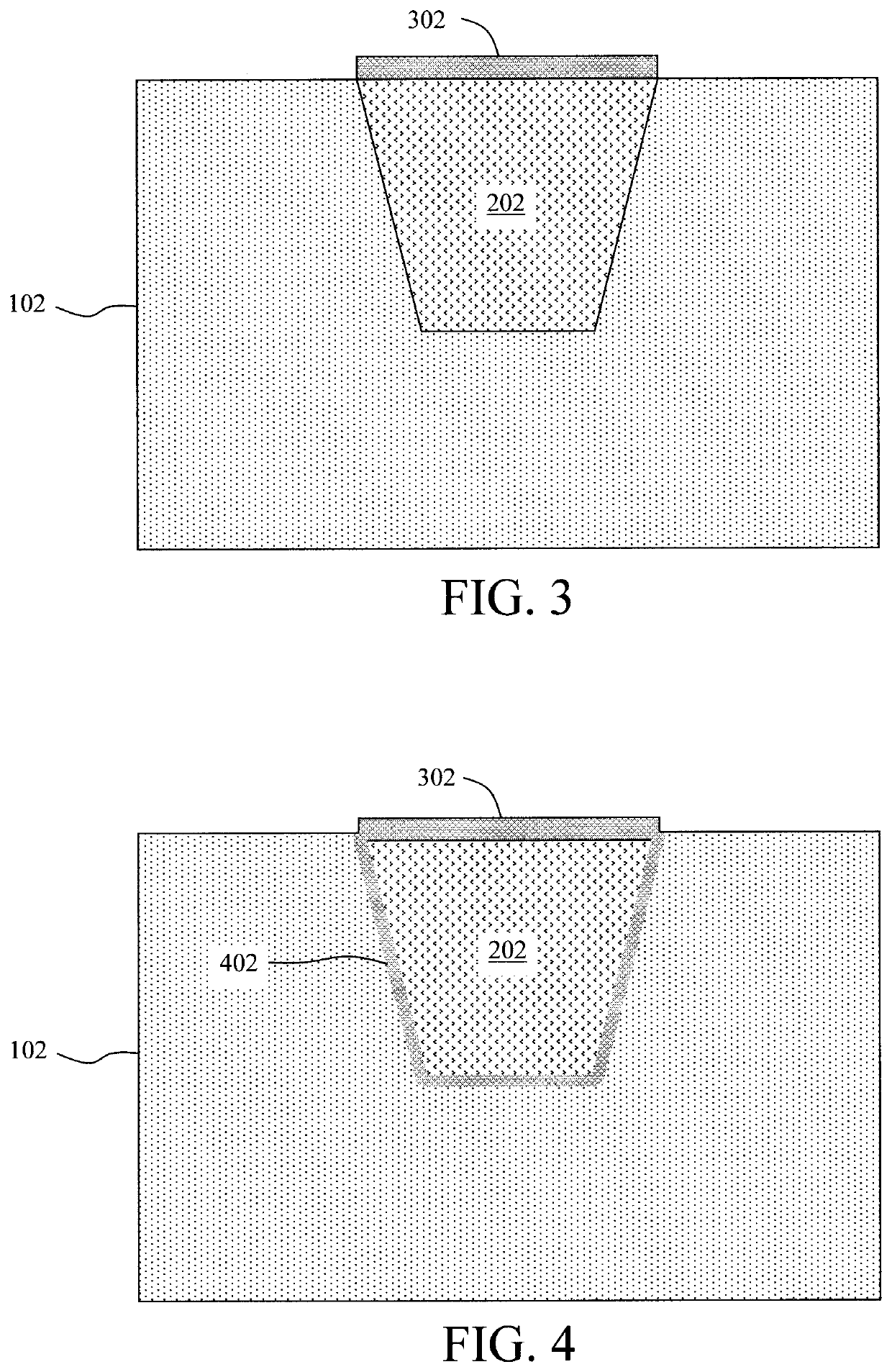
[0030]Provided herein are (e.g., cobalt (Co), ruthenium (Ru), etc.) interconnect structures with self-forming, wrap-all-around graphene barrier layer that surrounds the interconnect and techniques for the fabrication thereof. The interconnects are completely wrapped with a thin graphene layer. This graphene layer serves as a metal barrier and improves the interface scattering and resistance.

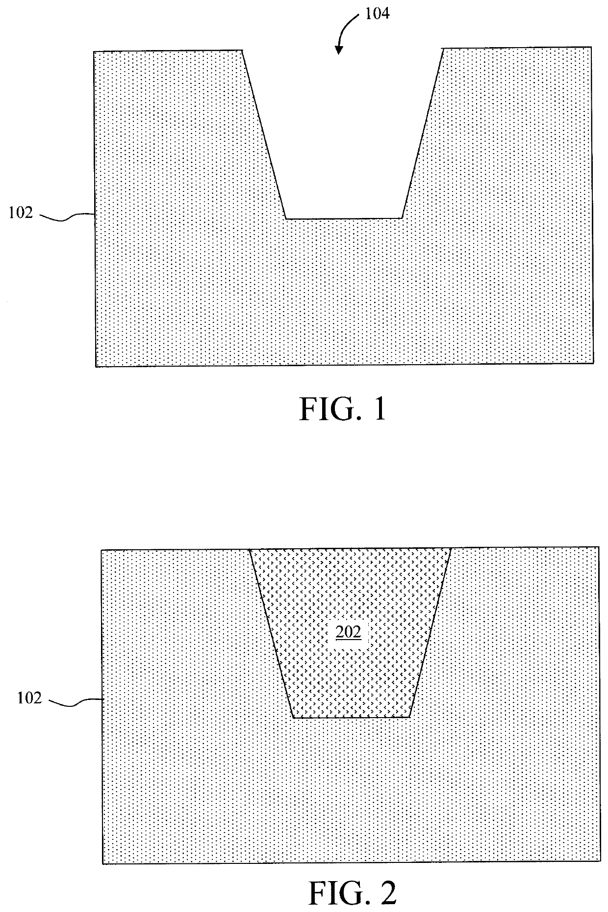
[0031]Several different process flows are provided herein to form the present interconnects with a wrap-all-around graphene barrier layer. For instance, in a first exemplary embodiment described by way of reference to FIGS. 1-4, carbon deposited on top of the interconnect is diffused to all buried metal-dielectric interfaces to form a thin graphene barrier layer that completely wraps around the interconnect.

[0032]Namely, as shown in FIG. 1, the process begins with a dielectric 102. Suitable dielectric materials include, but are not limited to, oxide materials such as silicon oxide (SiOx) and / or o...


PUM


Abstract

The present invention provides interconnects with self-forming wrap-all-around graphene barrier layer. In one aspect, a method of forming an interconnect structure is provided. The method includes: patterning at least one trench in a dielectric; forming an interconnect in the at least one trench embedded in the dielectric; and forming a wrap-all-around graphene barrier surrounding the interconnect. An interconnect structure having a wrap-all-around graphene barrier is also provided.

Description

FIELD OF THE INVENTION[0001]The present invention relates to interconnect technology, and more particularly, to interconnects with self-forming wrap-all-around graphene barrier layer.BACKGROUND OF THE INVENTION[0002]Traditionally, copper (Cu) has been used as the main interconnect conducting metal. However, as device dimensions shrink, the resistance of Cu-based interconnects becomes very high.[0003]Further, Cu interconnects require the use of a barrier layer to prevent diffusion of the Cu into the surrounding dielectric. Use of conventional barrier materials like titanium nitride (TiN), tantalum nitride (TaN), however, unduly limits the amount of Cu in the interconnect, thereby further increasing the resistance.[0004]Cobalt (Co) or other alternative metals can be used to replace Cu as the main interconnect conducting metal due to thinner or no liner requirements and shorter mean free path. However, metals like Co can still diffuse into the surrounding dielectric. Thus, a barrier is...

Claims


Application Information

Patent Timeline
IPC IPC(8): H01L21/768H01L23/522H01L23/532
CPCH01L21/76849H01L23/53276H01L21/76802H01L23/5329H01L21/76883H01L23/5226H01L21/76846H01L21/76864H01L23/53252H01L23/53209H01L21/76843H01L21/76867
Inventor HUANG, HUAINOGAMI, TAKESHIGRILL, ALFREDBRIGGS, BENJAMIN D.LANZILLO, NICHOLAS A.LAVOIE, CHRISTIANSIL, DEVIKABHOSALE, PRASADKELLY, JAMES
Owner IBM CORP
Learn More