

Substrate polishing device and substrate polishing method
- Summary
- Abstract
- Description
- Claims
- Application Information
AI Technical Summary
Benefits of technology
Problems solved by technology
Method used
Image

Examples
Embodiment Construction
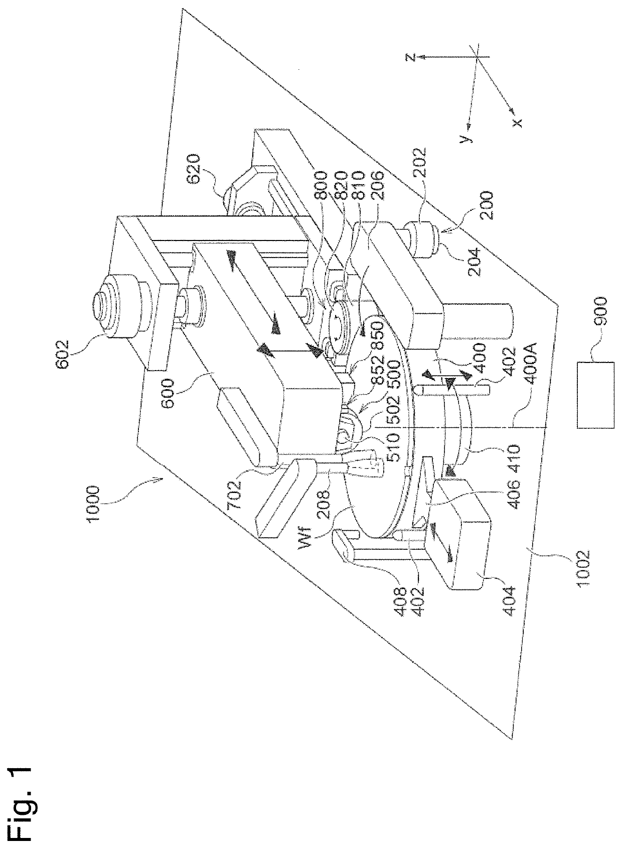
[0042]Embodiments of a partial polishing device according to the present invention will be described referring to the attached drawings. In the attached drawings, the same or similar components will be designated with the same or similar reference signs, and repetitive explanations of the embodiments, thus will be omitted from description of the respective embodiments. Features to be described in the respective embodiments may be applied to other embodiments so long as those features do not mutually conflict.
[0043]FIG. 1 is a schematic view showing a structure of a partial polishing device 1000 according to an embodiment. As FIG. 1 shows, the partial polishing device 1000 is formed on a base surface 1002. The partial polishing device 1000 may be formed as an independent device, or as a module constituting a substrate processing system 1100 including a large-diameter polishing device 1200 using a large-diameter polishing pad together with the partial polishing device 1000 (see FIG. 1...
PUM
 Abstract
Description
Claims
Application Information