

3D printer
a microelectronic printer and printer technology, applied in the direction of manufacturing tools, manufacturing enclosures, manufacturing driving means, etc., can solve the problems of inability to achieve full automatic, inability to produce a product, and inability to meet the requirements of flexible semiconductor device manufacturing
- Summary
- Abstract
- Description
- Claims
- Application Information
AI Technical Summary
Benefits of technology
Problems solved by technology
Method used
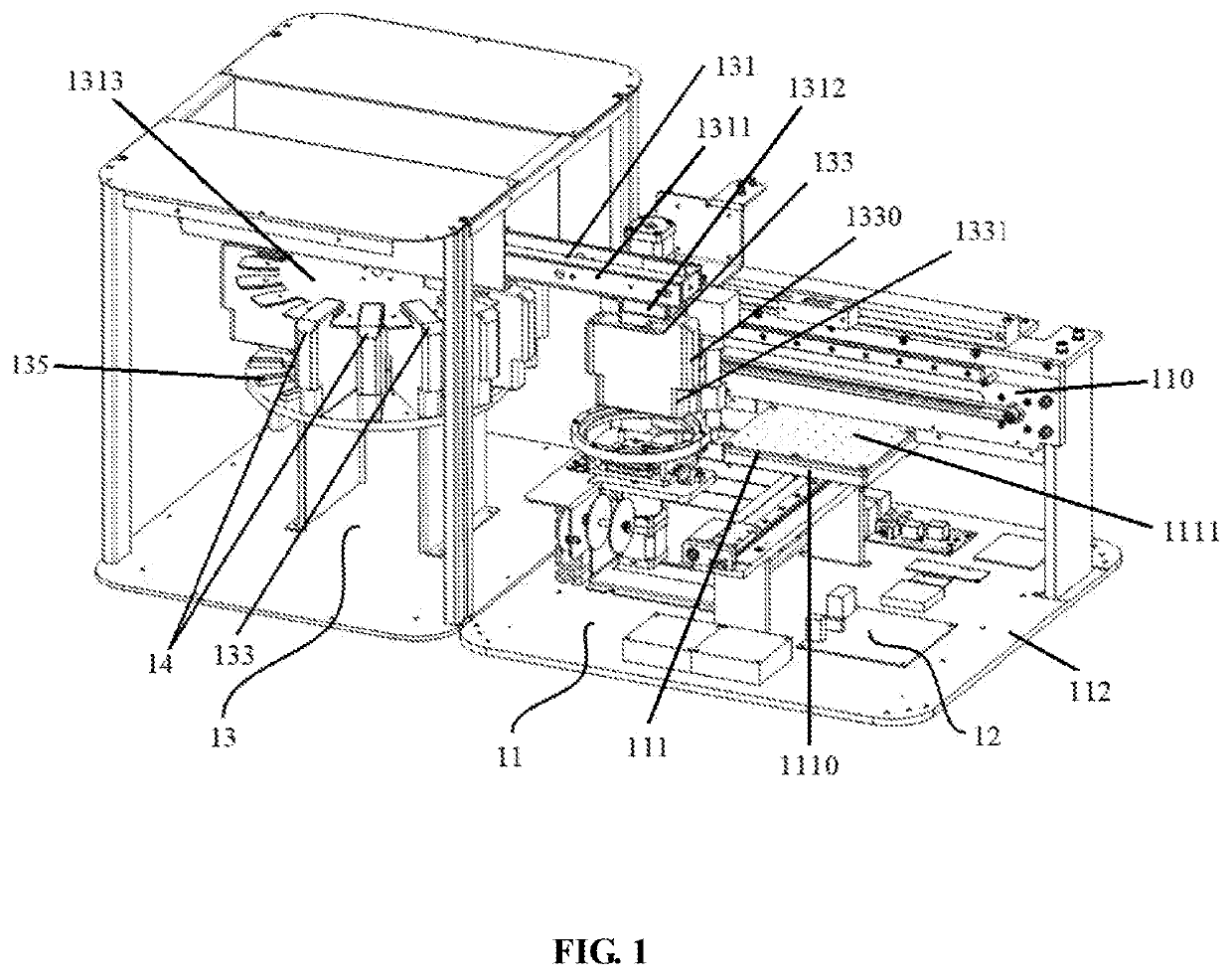
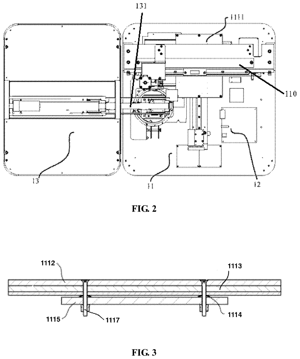
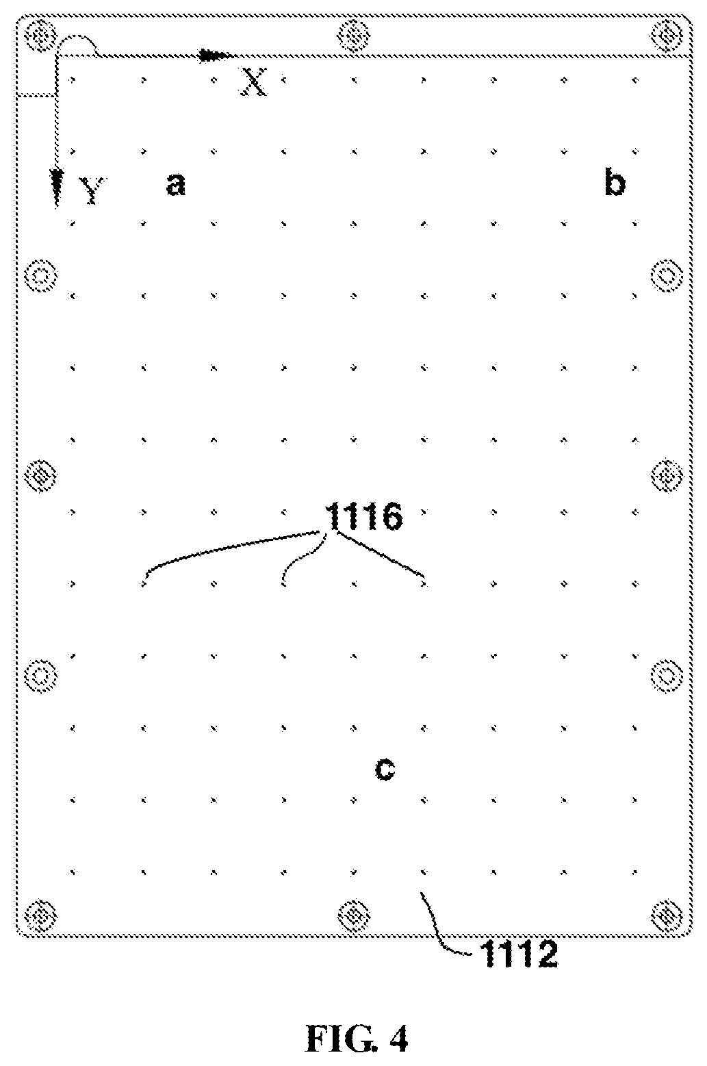
Image

Examples
Embodiment Construction
[0032]The present invention is described in details in the following embodiments, but the embodiments shall not be used to limit to the scope of protection for the invention.
[0033]In the present invention, “circuit” refers to a conductive loop formed by connecting at least one component or subcircuit through electrical or electromagnetic connection. When a component or circuit is referred to as “connected to” another component or the component / circuit is “connected” between the two nodes, it can be directly coupled or connected to the other component or intermediate components can be existed, and connections of components can be physical, logical, or a combination thereof. In contrast, when a component is referred to as “directly coupled” or “directly connected” to another component, it is meant that there are no intermediate components.
[0034]Unless clearly required by the context otherwise, “including,”“comprising,” and the like should be interpreted as meanings of contain rather t...
PUM
| Property | Measurement | Unit |
|---|---|---|
| temperature | aaaaa | aaaaa |
| diameter | aaaaa | aaaaa |
| pressure | aaaaa | aaaaa |
Abstract
Description
Claims
Application Information