Light emitting apparatus and electronic device comprising the same

Inactive Publication Date: 2020-10-08
DOW GLOBAL TECH LLC +1
View PDF0 Cites 0 Cited by
  • Summary
  • Abstract
  • Description
  • Claims
  • Application Information

AI Technical Summary

Benefits of technology

This patent describes a new light emitting device that uses blue LED technology and a special color conversion array made up of red, green, and blue nanoparticles. The nanoparticles are very small (measuring less than 100 nm) and can produce light with very specific colors. This technology can create high-quality colors with high purity levels, and it also reduces power consumption by about 50% compared to traditional color filter arrays. The design also simplifies the control system for the liquid crystal component.

Problems solved by technology

More importantly, such design could potentially lead to nearly 50% of power consumption reduction, relative to conventional color filter arrays.

Method used


Image

  • Light emitting apparatus and electronic device comprising the same
  • Light emitting apparatus and electronic device comprising the same
  • Light emitting apparatus and electronic device comprising the same

Examples


example 1

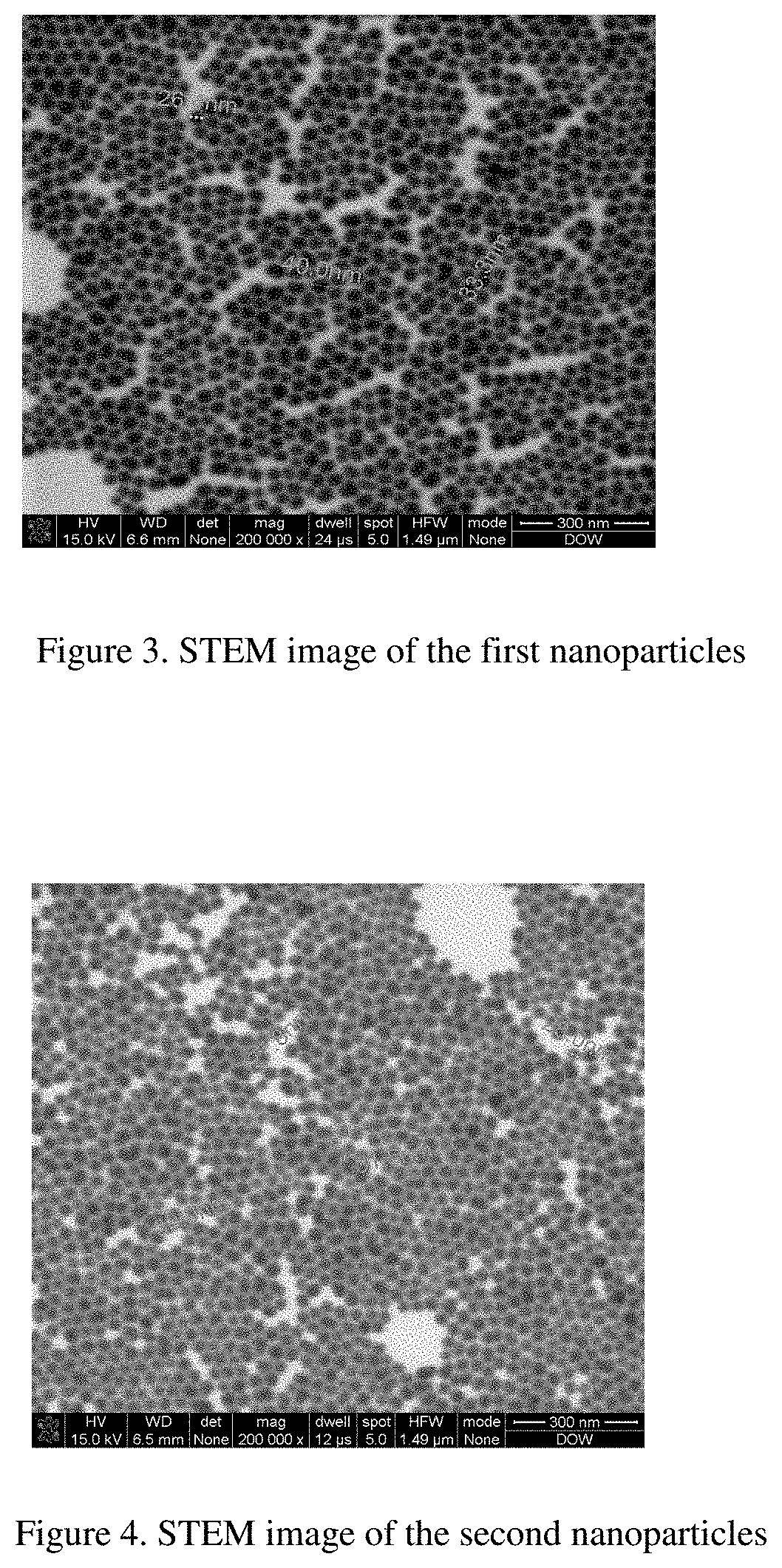
[0116]150 mg of the first nanoparticles obtained above were dissolved into 1 g of propylene glycol monomethyl ether acetate (PGMEA) to form a clear solution. The solution was then homogeneously mixed with 3 g of PMMA solution (30 wt % in PGMEA), coated onto a polyethylene terephthalate (PET) film, and then dried in an oven at 80° C. for 2 hours to evaporate PGMEA solvent. No barrier film or any tricks that would improve the barrier properties of the obtained first nanoparticles-PMMA film was used. The thickness of the dried film was around 80-100 μm. Storage stability and photostability properties of the first nanoparticles-PMMA film were determined according to the test method below.

[0117]Storage Stability

[0118]The storage stability test was conducted via the following steps: 1) Cut each nanoparticles-PMMA film sample into 4 pieces and place them in a humidity chamber; 2) Set the chamber at 90% of relative humidity (RH) and 60° C.; and 3) Every 100 hours, a sample piece was taken o...

example 2

[0121]The second nanoparticles-PMMA film was prepared according to the same procedure as described above for preparing the first nanoparticles-PMMA film of Example 1. Photostability of the second nanoparticles-PMMA film was evaluated according to the test method described above in Example 1.

[0122]Storage stability of the first nanoparticles-PMMA film (Example 1) was evaluated according to the test described above. It shows that 73% of the initial emission intensity of the first nanoparticles-PMMA film was maintained after 406 hour storage at 60° C. and 90% RH.

[0123]Table 2 gives photostability properties of films of Examples 1 and 2. As shown in Table 2, the first nanoparticles-PMMA and the second nanoparticles-PMMA films showed good photostability with about 82% and 100% retention of initial light intensity after 273 hours and 352 hours irradiation by blue backlight, respectively.

TABLE 2Photostability of nanoparticles-PMMA filmsunder blue backlight irradiationIrradiation% of initia...

example 3

[0124]150 mg of the first nanoparticles obtained above was dissolved into 1.2 g of PGMEA to form a clear solution. The solution was then homogeneously mixed with a photoresist binder developed for traditional color filters (Sample A acrylic binder (30 wt % in PGMEA), available from Showa Denko) and 9 mg of a photo initiator OXE-02. After thorough mixing, the mixture was coated onto a glass substrate via spin coating and then pre-baked in an oven at 100° C. for 2 minutes. The resulted film was irradiated under 365 nm UV with an intensity of 50 mJ / cm2, followed by baking at 230° C. for 30 minutes twice. The photoluminescence spectrum of the sample was recorded before and after each step with spectrofluorometer (HORIBA FluoroMax-4). Stability of the first nanoparticles under UV curing and hard-baking conditions is given in Table 3.

[0125]Table 3 shows the stability performance of first nanoparticles in the acrylic binder towards the UV curing and hard-baking conditions commonly used for...


PUM


Abstract

A light emitting apparatus affording high quality colors and energy economy and an electronic device comprising the light emitting apparatus.

Description

FIELD OF THE INVENTION[0001]The present invention relates to a light emitting apparatus and an electronic device comprising the same.INTRODUCTION[0002]Conventional liquid crystal display (LCD) devices include an LCD unit and a backlight unit which uniformly illuminates the LCD unit with white light. A main factor that determines the maximum color performance of LCD devices is the spectral interaction between the light emitted from the backlight unit and the color filter array of the LCD unit. The color filter array consists of millions of individually addressable pixels, each of which are made up of red (R), green (G) and blue (B) sub-pixels.[0003]A major problem of conventional LCD devices is the large light loss associated with the LCD unit above the backlight source. Typically only less than 10% of light emitted from the backlight source is used and the remaining over 90% is absorbed by the LCD unit, including a polarizing filter, a thin film transistor (TFT) array, a liquid crys...

Claims


Application Information

Patent Timeline
IPC IPC(8): C09K11/06C07F7/18H01L51/00C09K11/02H01L27/32H01L27/15G02F1/13357
CPCH01L27/15C09K11/06C07F7/1804C09K11/025G02F1/133617H01L51/0053H01L27/322H01L51/0094C09K2211/1018G02F2202/36C09K11/0838C09K2211/1055C09K2211/1044C09K2211/1007C09K2211/1011C09K2211/1029C09K2211/1088H01L33/504G02B5/201G02F1/133614H10K59/38H10K85/40H10K85/621
Inventor WANG, XIUYANLI, YANGREN, XIAOFANLV, BOHU, NANTREFONAS, III, PETERKIM, YONGCHEOLHUANG, YAN
Owner DOW GLOBAL TECH LLC
Why Eureka
Try Eureka