

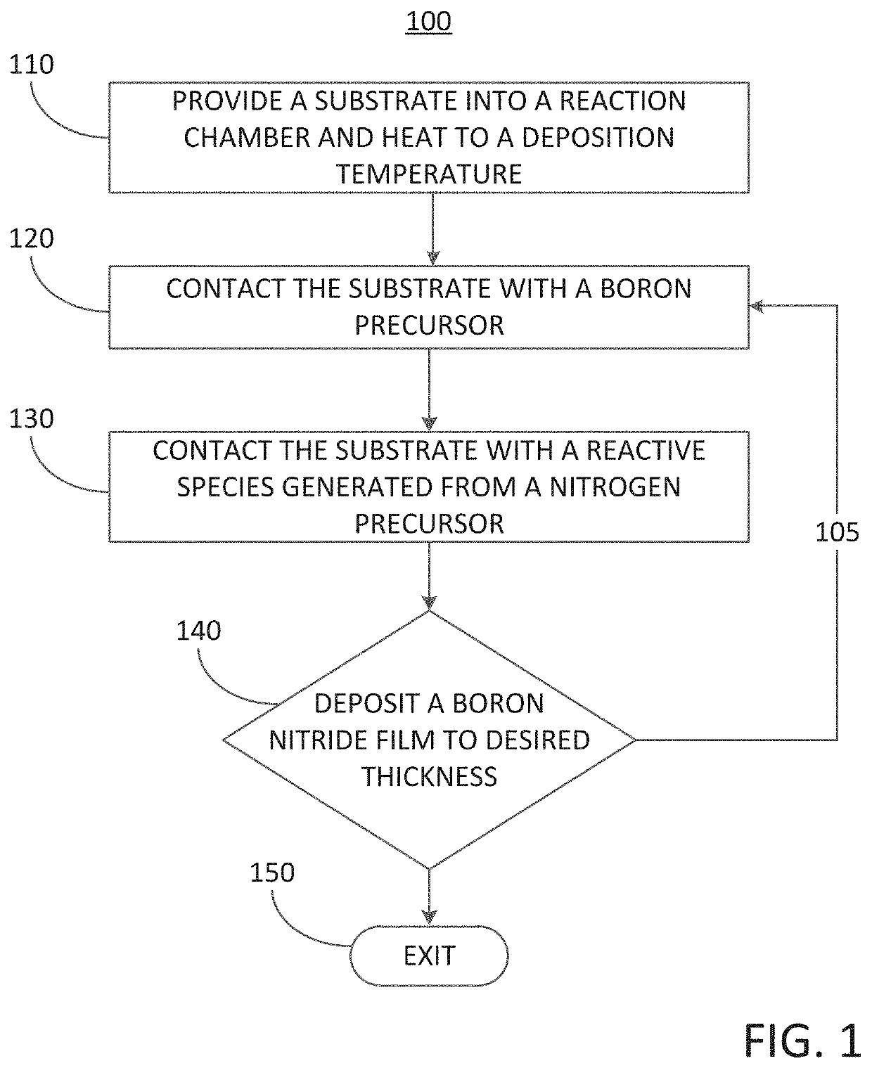
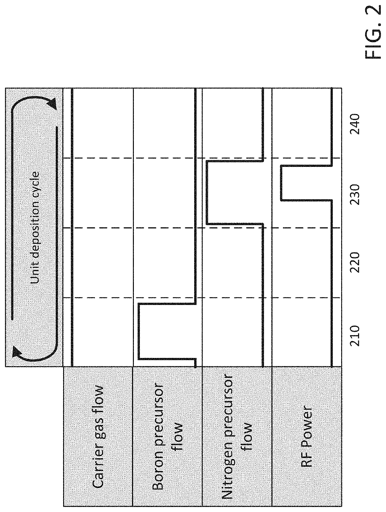
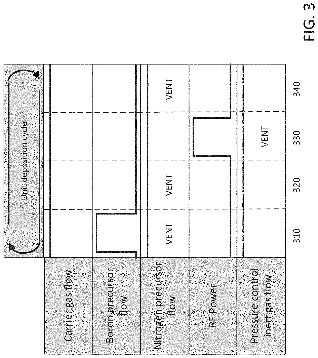
Methods for forming a boron nitride film by a plasma enhanced atomic layer deposition process
a technology of boron nitride and atomic layer, which is applied in the direction of chemical vapor deposition coating, metal material coating process, coating, etc., can solve the problems of non-conformal films which may be unsuitable for non-planar substrates including high aspect ratio features
- Summary
- Abstract
- Description
- Claims
- Application Information
AI Technical Summary
Benefits of technology
Problems solved by technology
Method used
Image

Examples
Embodiment Construction
[0014]Although certain embodiments and examples are disclosed below, it will be understood by those in the art that the invention extends beyond the specifically disclosed embodiments and / or uses of the invention and obvious modifications and equivalents thereof. Thus, it is intended that the scope of the invention disclosed should not be limited by the particular disclosed embodiments described below.
[0015]As used herein, the term “substrate” may refer to any underlying material or materials that may be used, or upon which, a device, a circuit or a film may be formed.
[0016]As used herein, the term “film” and “thin film” may refer to any continuous or non-continuous structures and material deposited by the methods disclosed herein. For example, “film” and “thin film” could include 2D materials, nanolaminates, nanorods, nanotubes, or nanoparticles or even partial or full molecular layers or partial or full atomic layers or clusters of atoms and / or molecules. “Film” and “thin film” ma...
PUM
| Property | Measurement | Unit |
|---|---|---|
| Temperature | aaaaa | aaaaa |
| Pressure | aaaaa | aaaaa |
| Ratio | aaaaa | aaaaa |
Abstract
Description
Claims
Application Information