Metal nanoparticle enhanced semiconductor film for functionalized textiles

a technology of functionalized textiles and semiconductor films, applied in the field of surface coatings, can solve the problems uniform film, and less readily removed fabric, and achieve the effects of less photocatalytic activity than a thin film, limited self-cleaning, anti-microbial, radiation-protective properties, and limited current methods and techniques

Pending Publication Date: 2020-10-15
BOARD OF RGT THE UNIV OF TEXAS SYST
View PDF0 Cites 0 Cited by
  • Summary
  • Abstract
  • Description
  • Claims
  • Application Information

AI Technical Summary

Benefits of technology

[0006]The method and system of this invention center around the innovative concept of methods for generating a nanostructured photocatalytic system on at least one surface of a material, for example a textile material, using simple, scalable methods. The invention allows a nanostructured photocatalytic system to be constructed using a sol-gel based synthetic method for depositing a semiconducting thin film that coats the fabric, provides a surface for photocatalytic chemical reactions to occur, and itself absorbs UV light preventing the penetration of the material by UV radiation. Noble metal nanoparticles are grown on this semiconducting surface by a solution-based coating method followed by irradiation with UV light which, together with the already deposited semiconducting layer, acts to reduce the noble metal precursors, and generate nanoparticles on the semiconducting surface. These nanoparticles are variably sized, which allows for the absorption (and thus the photochemical utilization) of a range of incident radiation that wouldn't be absorbed by the semiconducting oxide layer alone. These nanoparticles are also capable as acting as electron acceptors for the photo-generated electrons from the oxide surface, which absorbs incident high-energy UV radiation. The nanoparticles thus help to reduce charge recombination and also generate additional excitons from the absorption of incident light at a longer wavelength than that absorbed by the semiconducting material. The tandem semiconducting oxide layer / nanoparticle system exhibits more efficient photocatalytic performance than other methods, and the synthetic techniques used in this invention are facile and scalable.
[0008]According to one embodiment of the present invention, this method provides a means for the large-scale facile manufacture of textile materials with said coating, which lends the finished materials self-cleaning, antimicrobial, and UV-protective properties.
[0009]According to one embodiment of the present invention, a method is provided for the direct reduction of gold chloride and silver nitrate (gold and silver nanoparticle precursors) on the semiconducting surface under intense UV radiation during the manufacturing process, thus enabling the direct growth of the nanoparticles on the oxide surface and improving manufacturing time compared to the utilization of various chemical reducing agents and / or the separate growth of the nanoparticles and subsequent deposition onto the semiconductor-coated fabric, which would further complicate manufacture.
[0010]According to one embodiment of the present invention, a method is provided for coating all fibrous / non-fibrous textile materials with a semiconducting layer and nanoparticles to lend them anti-microbial, self-cleaning, and radiation-protective properties.
[0011]The present invention advances the art of treating textile materials with the aim of obtaining a textile material that has self-cleaning, anti-microbial, or radiation protective properties, and, in addition, provides an improved method for the application of the coating in a scalable manufacturing process.

Problems solved by technology

Treatment methods that rely on semiconducting materials being deposited on a textile typically rely on complicated methods ill-suited to scaling to industrial scale, and also typically yield a textile material that is impregnated by and / or decorated with discrete semiconductor nanotubes or nanoparticles, which both have the disadvantage of being more readily removed from the fabric and less photocatalytically active than a thin, uniform film.
While advancements have been made in the development of advanced textile materials with a photocatalytic film or layer, current methods and techniques are inadequate because they are ill-suited to large scale production and they have limited self-cleaning, anti-microbial, and radiation-protective properties.

Method used


Image

  • Metal nanoparticle enhanced semiconductor film for functionalized textiles
  • Metal nanoparticle enhanced semiconductor film for functionalized textiles
  • Metal nanoparticle enhanced semiconductor film for functionalized textiles

Examples


Embodiment Construction

[0029]The invention will now be described with reference to the drawing figures, in which like reference numerals refer to like parts throughout. For purposes of clarity in illustrating the characteristics of the present invention, proportional relationships of the elements have not necessarily been maintained in the drawing figures.

[0030]The following detailed description of the invention references specific embodiments in which the invention can be practiced. The embodiments are intended to describe aspects of the invention in sufficient detail to enable those skilled in the art to practice the invention. Other embodiments can be utilized and changes can be made without departing from the scope of the present invention. The present invention is defined by the appended claims and the description is, therefore, not to be taken in a limiting sense and shall not limit the scope of equivalents to which such claims are entitled.

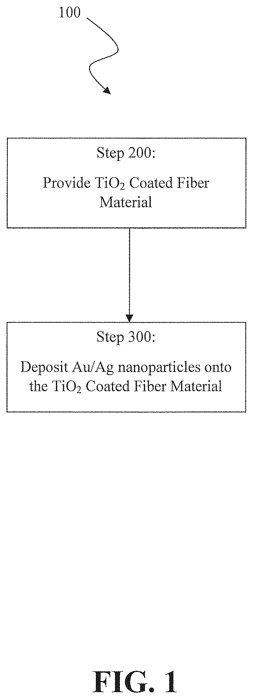
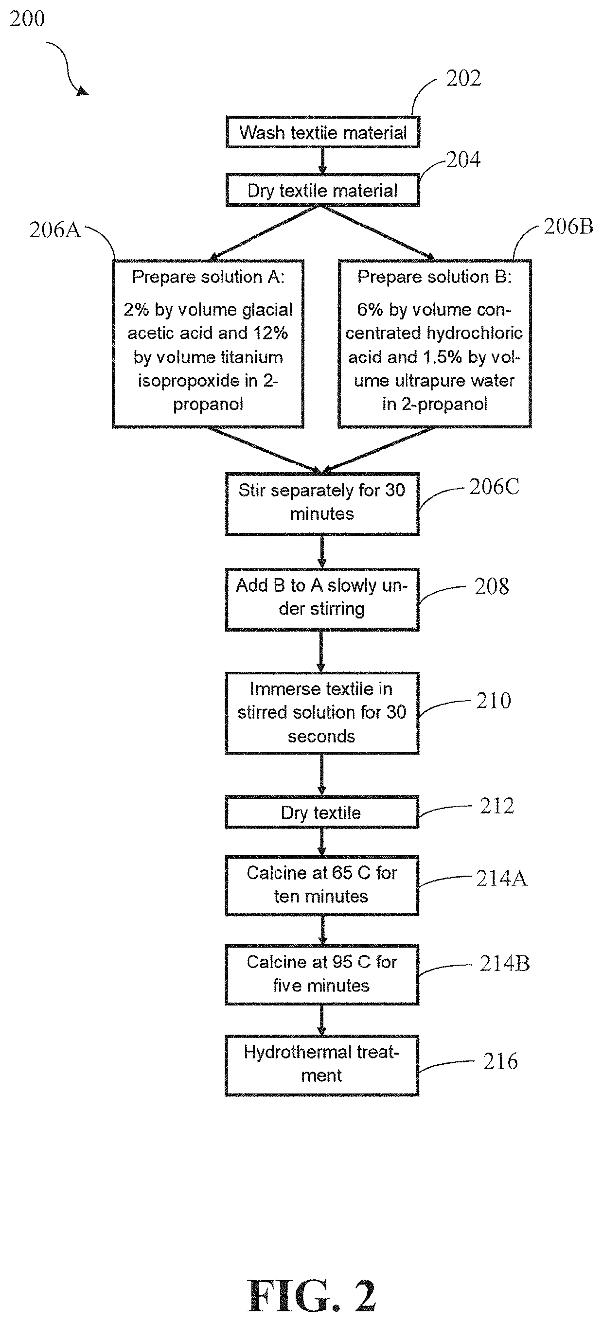
[0031]The present invention is directed to gold and / or silv...


PUM

PropertyMeasurementUnit
time periodaaaaaaaaaa
sizeaaaaaaaaaa
sizeaaaaaaaaaa

Abstract

A method for forming a metallic nanoparticle and semiconductor coated fiber material is provided. The method can include the steps of coating at least one surface of a material, for example a textile material, with a semiconducting layer, and growing metallic nanoparticles on the semiconducting layer. The steps for coating the surface of the material with a semiconducting layer can include forming a titanium dioxide film on the surface of the textile material. The steps for forming metallic nanoparticles on a semiconducting layer can include immersing the coated textile layer in a metallic nanoparticle precursor solution, drying the coated textile layer and exposing the textile layer to UV radiation. The metallic nanoparticles can include gold and / or silver nanoparticles. Also disclosed are materials having a least one treated surface coated with metallic nanoparticles. The treated surface may comprise the surface of a textile material treated according to the methods provided herein.

Description

GOVERNMENT LICENSE RIGHTS[0001]This invention was made with government support under D01_W911SR-14-2-0001-0003 awarded by the Department of Defense. The government has certain rights in the invention.CROSS REFERENCE TO RELATED APPLICATIONS[0002]NoneFIELD OF THE INVENTION[0003]This invention relates to the field of surface coatings and methods for providing a surface coating to a material, as a method of treating a material, for example a textile material, such that at least one surface of the material comprises a nanostructured coating is provided. The invention also relates to the field of nanostructured coatings that are self-cleaning, anti-microbial, and radiation-protective. The invention further relates to the field of semiconducting metal oxide thin film coatings, as semiconducting metal oxide thin film coating comprising metallic nanoparticle incorporated to a semiconducting film is provided, the film providing an active photocatalyst layer imparting the above characteristics...

Claims


Application Information

Patent Timeline
Patent Type & Authority Applications(United States)
IPC IPC(8): D06M11/83D06M16/00
CPCD06M16/00D06M11/83D06M2200/01A41D31/30A41D13/1192D06M2101/06D06M2200/00D06M2400/02A41D13/1161
Inventor UDDIN, MOHAMMED JASIMJAKSIK, JAREDMOORE, H. JUSTIN
Owner BOARD OF RGT THE UNIV OF TEXAS SYST
Why Eureka
Try Eureka