
Transistorless all-memristor neuromorphic circuits for in-memory computing

a neuromorphic circuit and all-memristor technology, applied in computing models, biological models, instruments, etc., can solve the problems of inability to multi-layer stackability, inconvenient multi-layer stacking, and large overheads

Pending Publication Date: 2020-11-12
HRL LAB
View PDF0 Cites 4 Cited by
  • Summary
  • Abstract
  • Description
  • Claims
  • Application Information

AI Technical Summary

Benefits of technology

The patent describes a neuromorphic crossbar array circuit that can perform multiply-accumulate arithmetic operations using spike-based neurons. The circuit includes a crossbar array with programmable conductance circuits connected between row and column lines. The circuit can be programmed to perform different operations and can be used for data processing and machine learning. The technical effects of the patent include improved performance and efficiency of the crossbar array circuit and the ability to program the circuit for different operations.

Problems solved by technology

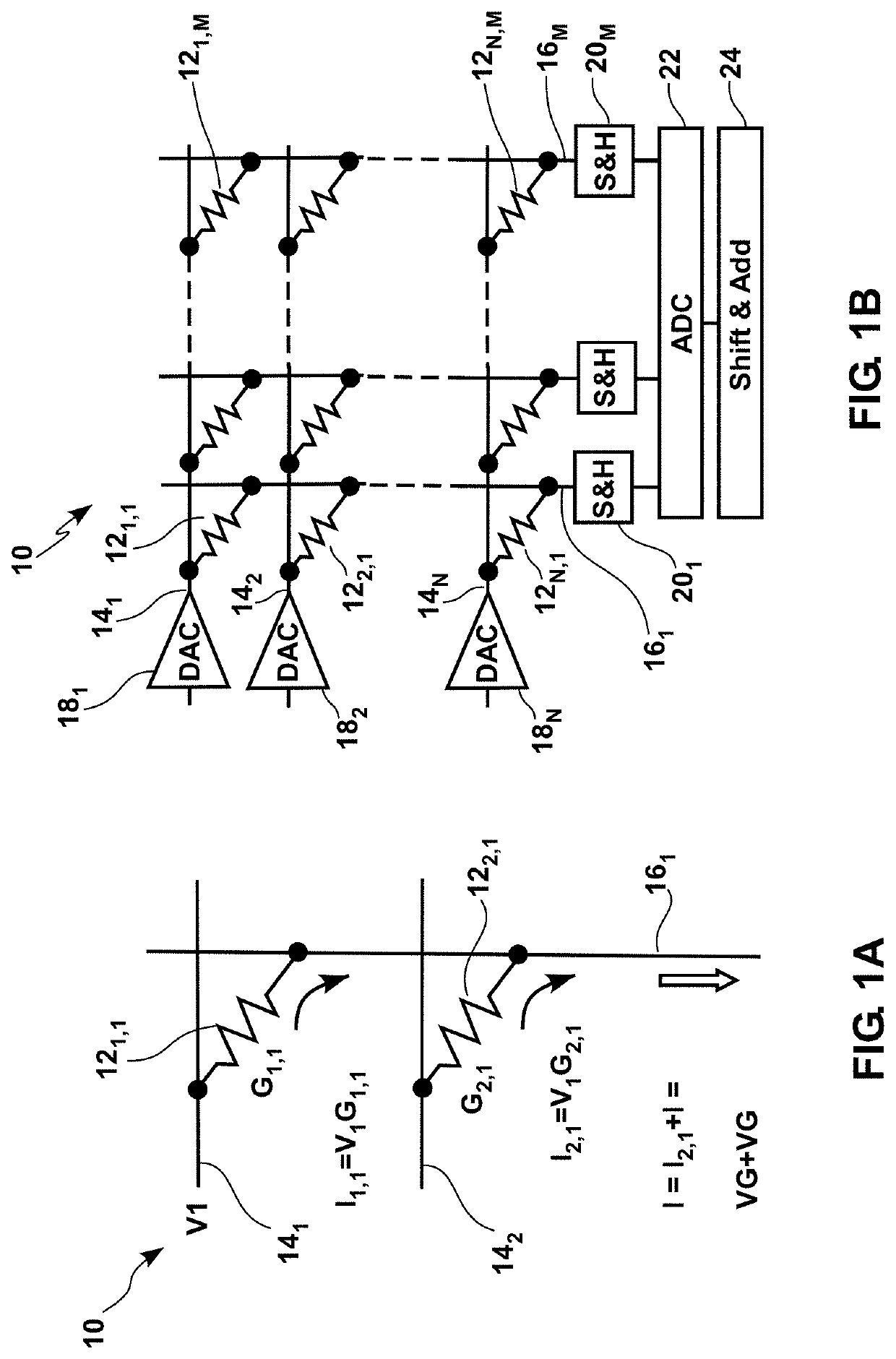
Although hybrid CMOS-memristor dot-product accelerators such as illustrated in FIG. 1B can realize analog domain computation in a parallel fashion, they face several challenges.
One challenge is that the interfacing / communication with the external digital circuitries necessitates the use of ADCs and DACs, as illustrated, which incur area and energy overheads.
Moreover, most of the demonstrations still require access transistors (1T1M / 1T1R, or one-transistor one-memristor / resistor cells) to block the sneak paths, hence preclude a multilayer stackability.

Method used


Image

  • Transistorless all-memristor neuromorphic circuits for in-memory computing
  • Transistorless all-memristor neuromorphic circuits for in-memory computing
  • Transistorless all-memristor neuromorphic circuits for in-memory computing

Examples


Embodiment Construction

[0074]The detailed description set forth below in connection with the appended drawings are intended as a description of various embodiments of the present invention and are not intended to represent the only embodiments in which the present invention is to be practiced. Each embodiment described in this disclosure is provided merely as an example or illustration of the present invention, and should not necessarily be construed as preferred or advantageous over other embodiments. In some instances, well-known methods, procedures, objects, and circuits have not been described in detail so as to not unnecessarily obscure aspects of the present disclosure.

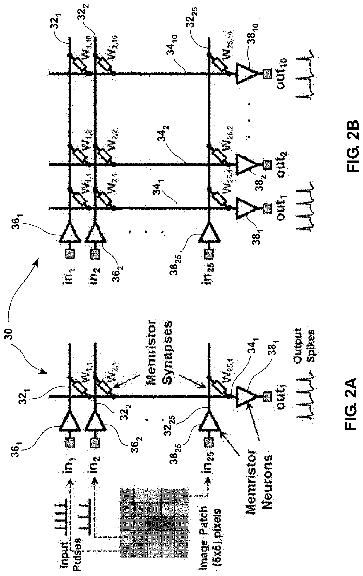
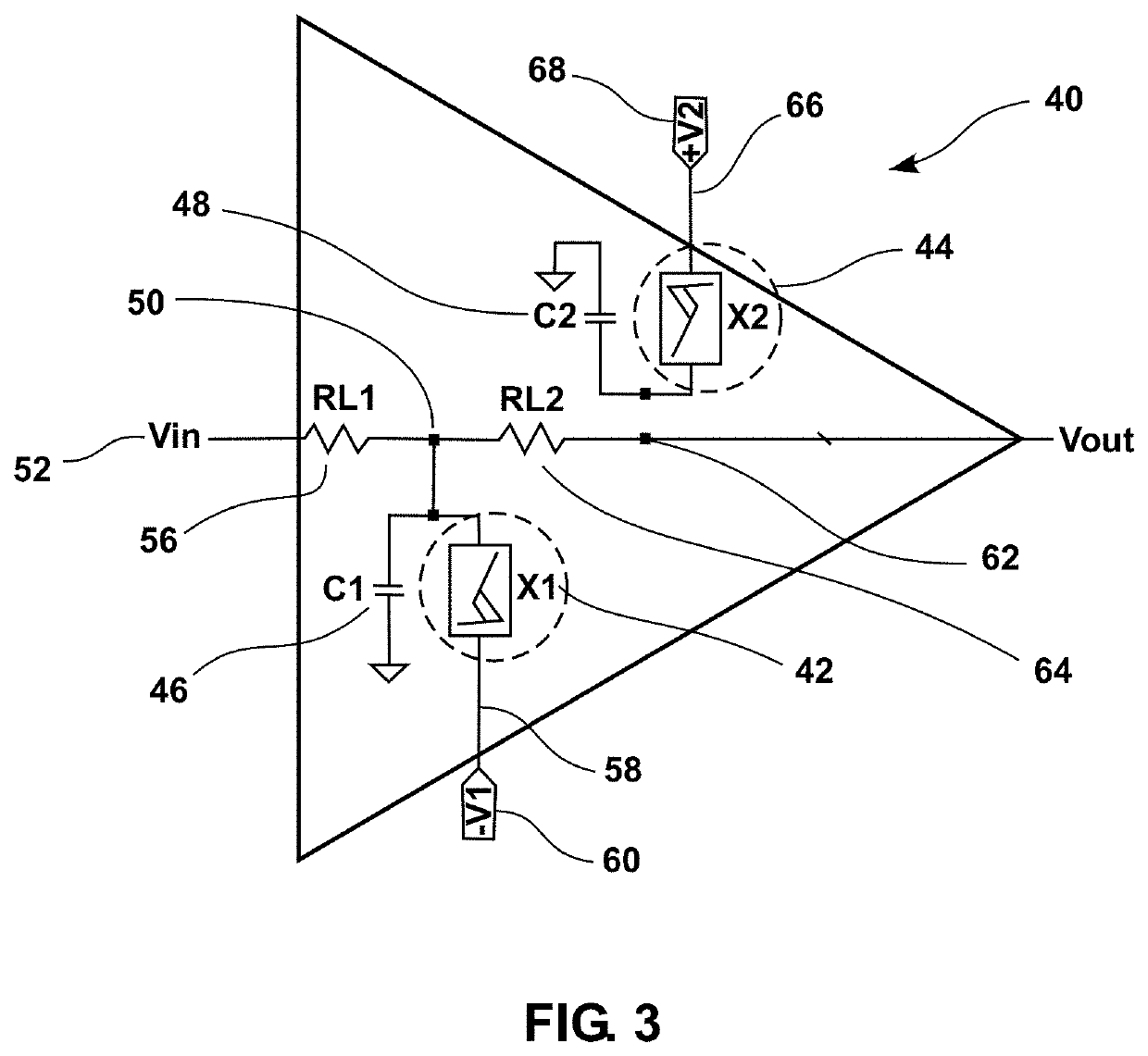
[0075]By contrast with the above-described prior art circuits, embodiments of this presentation relate to an all-memristor neuromorphic MAC accelerator that can be entirely analog, which can employ nonvolatile passive-memristor synapses for row-to-column coupling, and spiking active-memristor neurons for generating input and output si...


PUM


Abstract

A circuit for multiplying a number N of first operands each by a corresponding second operand, and for adding the products of the multiplications, with N≥2; the circuit comprising: N input conductors; N programmable conductance circuits connected each between one of the input conductors and at least one output conductor; each programmable conductance circuit being arranged to be programmable at a value depending in a known manner from one of the first operands; each input conductor being arranged to receive from an input circuit an input train of voltage spikes having a spike rate that derives in a known manner from one of the second operands; and at least one output circuit arranged to generate an output train of voltage spikes having a spike rate that derives in a known manner from a sum over time of the spikes received on the at least one output conductor.

Description

CROSS REFERENCE TO RELATED APPLICATIONS[0001]This application is related to and claims priority from U.S. Provisional Application Ser. No. 62 / 844,611, filed May 7, 2019. This application is related to and claims priority from U.S. Provisional Application Ser. No. 62 / 860,915, filed Jun. 13, 2019. This application is related to U.S. Non-Provisional Application (NP 632100 in prep), which is incorporated by reference herein as though set forth in full.STATEMENT REGARDING FEDERAL FUNDING[0002]This invention was made under U.S. Government contract FA8650-18-C-7869. The U.S. Government has certain rights in this invention.FIELD OF THE INVENTION[0003]Embodiments of the present technology relate generally to a device and method to conduct fast and energy-efficient Multiply-ACcumulate (MAC) arithmetic operations; in particular Vector-Matrix Multiplication (VMM) operations in a parallel fashion.BACKGROUND[0004]One way to implement VMM operations in hardware is an architecture known as a crossb...

Claims


Application Information

Patent Timeline
IPC IPC(8): G06N3/063G06F17/16
CPCG06F17/16G06N3/0635H01L27/2463G06F7/5443G06F2207/4824G06F2207/4802G11C11/54G11C13/0002G11C2213/77G11C7/1006G06N3/049G06N3/084G06N3/065G06N3/045G06N3/0464G06N3/09G06N3/048G06F17/15G11C11/34H10B63/80
Inventor YI, WEICRUZ-ALBRECHT, JOSE
Owner HRL LAB
Learn More