TFT substrate, ESD protection circuit and manufacturing method of TFT substrate

a technology of protection circuit and substrate, which is applied in the direction of semiconductor devices, circuit arrangements, instruments, etc., can solve the problems of affecting the production yield, and esd, so as to avoid the abnormality of the lcd screen and the leakage current is small.

Inactive Publication Date: 2020-11-19
SHENZHEN ROYOLE TECH CO LTD
View PDF0 Cites 0 Cited by
  • Summary
  • Abstract
  • Description
  • Claims
  • Application Information

AI Technical Summary

Benefits of technology

[0040]In the implementation of the technical solution of the present invention, since the TFT substrate adopts a double gate structure, and the second gate is connected to a negative voltage, the turn-on voltage of the TFT transistor can be shifted to a positive direction. Moreover, when the TFT transistor is used to construct the ESD protection circuit, even if static electricity occurs, since the turn-on voltage of both TFT transistors is greater than 0, the leakage current is very small and can be ignored. In this way, the data signal output from the driver IC will not be doped with undesired voltage signal, so that the brightness of pixel electrode will not occur abnormal conditions, thereby avoiding the abnormality of the LCD screen.

Problems solved by technology

However, in the manufacturing process of the liquid crystal display substrate, multiple processes such as development, etching, liquid crystal alignment into a cell, and transportation may cause electro-static discharge (ESD).
The charge generated by static electricity will damage the TFT transistor device and the insulating layer, resulting in the degradation of the liquid crystal panel and affecting the production yield.
However, in this ESD protection circuit, due to the poor uniformity distribution of the initial turn-on voltage on the TFT transistor process, the initial turn-on voltage of the TFT transistor in actual products will move to a negative voltage, which means, the initial turn-on voltage of the TFT transistor is lower than 0.
When the data signal is used to drive the pixel electrode, since the data signal is doped with an undesirable voltage, the brightness of the pixel electrode will be abnormal, thereby causing abnormality in the screen displayed by the liquid crystal panel.

Method used


Image

  • TFT substrate, ESD protection circuit and manufacturing method of TFT substrate
  • TFT substrate, ESD protection circuit and manufacturing method of TFT substrate
  • TFT substrate, ESD protection circuit and manufacturing method of TFT substrate

Examples


Embodiment Construction

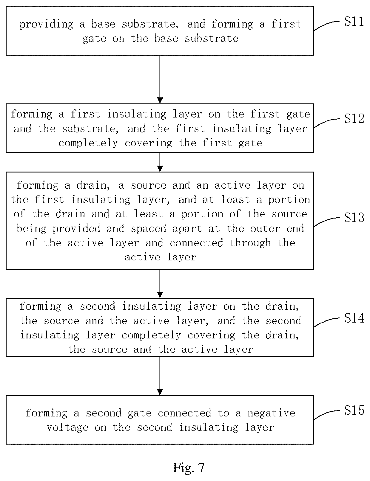
[0049]In the following, the technical solutions in the embodiments of the present invention will be clearly and completely described with reference to the drawings in the embodiments of the present invention. Obviously, the described embodiments are only a part of the embodiments of the present invention, but not all of the embodiments. Based on the embodiments of the present invention, all other embodiments obtained by an ordinary person of skill in the art without creative efforts shall fall within the scope of protection of the present invention.

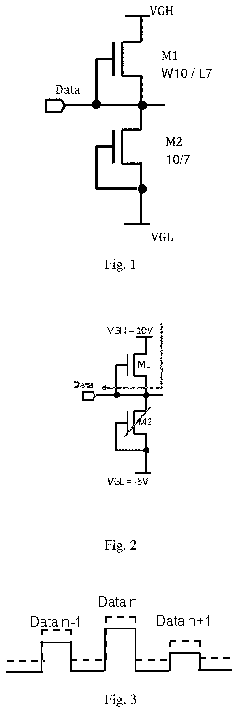
[0050]FIG. 4 is a schematic structural view of the embodiment 1 of the TFT substrate of the present invention. The TFT substrate of this embodiment comprises a stacked arrangement of a base substrate 11, a first gate 12, a first insulating layer 13, a drain 14, a source 15, an active layer 16, a second insulating layer 17, a the second gate 18. Wherein, the first gate 12 is provided on the base substrate 11 and has an area smaller than th...


PUM

PropertyMeasurementUnit
turn-on voltageaaaaaaaaaa
negative voltageaaaaaaaaaa

Abstract

A TFT substrate, an ESD protection circuit, and a method for manufacturing the TFT substrate. The TFT substrate comprises: a base substrate; a first gate provided on the base substrate; a first insulating layer provided on the first gate; a drain, a source, and an active layer provided on the first insulating layer; a second insulating layer provided on the drain, the source, and the active layer; and a second gate provided on the second insulating layer. In this way, display abnormality of a liquid crystal panel screen can be avoided.

Description

RELATED APPLICATION[0001]The present application is a U.S. National Phase of International Application Number PCT / CN2017 / 113151, filed Nov. 27, 2017.TECHNICAL FIELD[0002]The invention relates to the field of liquid crystal display, in particular to a TFT substrate, an ESD protection circuit and a manufacturing method of TFT substrate.BACKGROUND TECHNIQUE[0003]Since TFT-LCD (Thin Film Transistor Liquid Crystal Display) has the advantages of light, thin, low power consumption, etc., it is widely used in equipments such as televisions, notebook computers, mobile phones, etc..[0004]As a flat panel display device, the liquid crystal panel of a liquid crystal display is usually composed of two glass substrates and a liquid crystal layer between the glass substrates. A number of data lines and a number of scanning lines are integrated on the lower glass substrate, and they are vertically staggered to form a number of unit areas, which are defined as pixel units. Each pixel unit mainly comp...

Claims


Application Information

Patent Timeline
Patent Type & Authority Applications(United States)
IPC IPC(8): H01L27/02H01L27/12
CPCH01L27/1214H01L27/0292H01L27/027H01L27/127G09G3/36H01L27/0266H01L27/0296H01L29/78645H01L29/78648H01L27/02H02H9/04H01L29/41733H01L29/42384
Inventor KIM, JI HA
Owner SHENZHEN ROYOLE TECH CO LTD
Why Eureka
Try Eureka