

Method for inspecting surface of wafer, device for inspecting surface of wafer, and manufacturing method of electronic component
a technology for inspecting the surface of wafers and manufacturing methods, applied in semiconductor/solid-state device testing/measurement, instruments, material analysis, etc., can solve the problem of taking a long time to determine foreign matter
- Summary
- Abstract
- Description
- Claims
- Application Information
AI Technical Summary
Benefits of technology
Problems solved by technology
Method used
Image

Examples
first embodiment
Surface Inspection Device
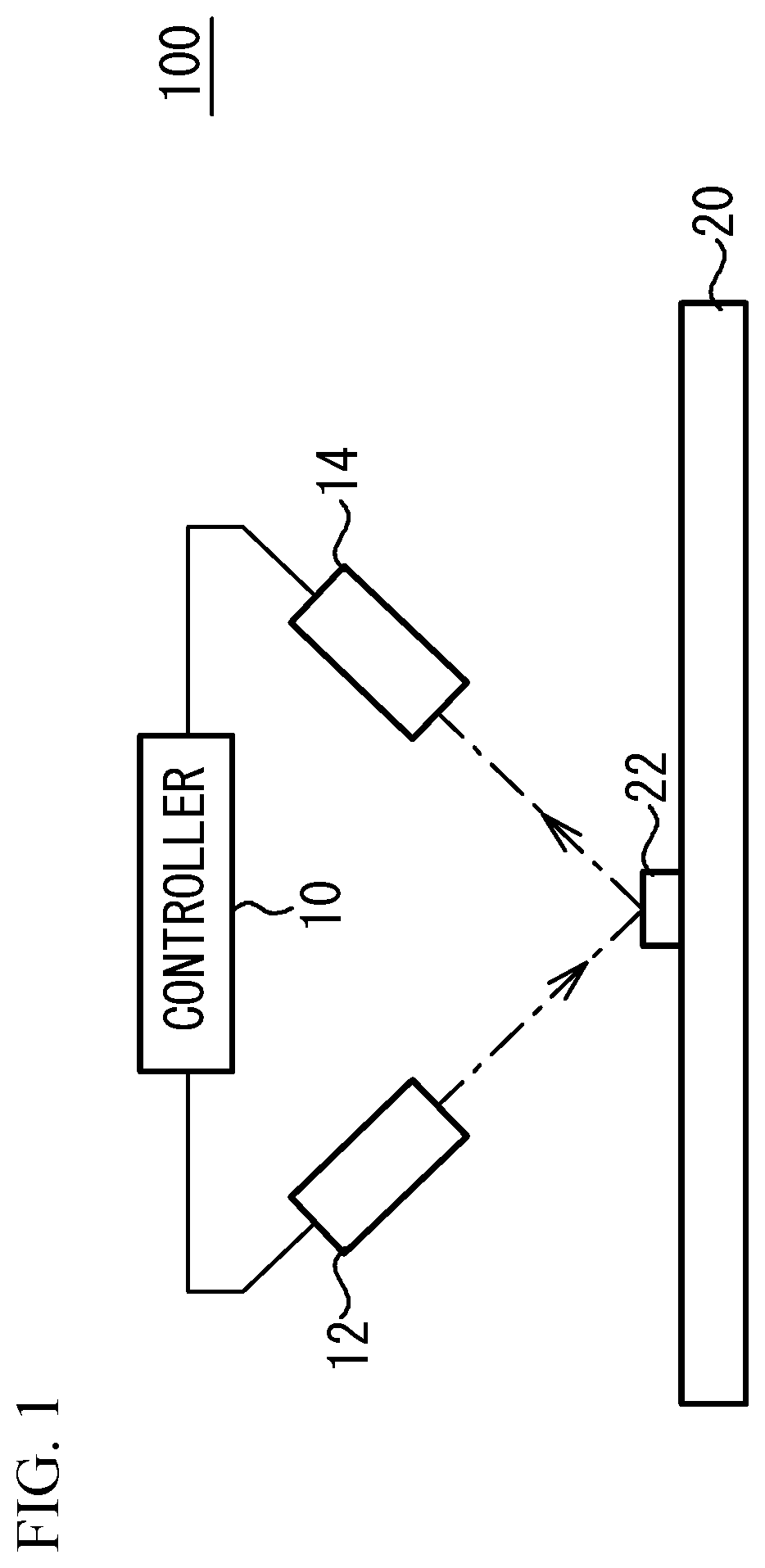
[0027]FIG. 1 schematically illustrates a surface inspection device 100 in accordance with a first embodiment. As illustrated in FIG. 1, the surface inspection device 100 includes a controller 10, a laser source 12, and a detector 14. The object that is subject to inspection is a wafer 20, and a foreign matter 22 may adhere to the surface of the wafer 20.
[0028]The laser source 12 is a semiconductor laser including, for example, gallium indium phosphorus (GaInP) and aluminum gallium indium phosphorus (AlGaInP). The oscillation wavelength of the laser source 12 can be adjusted by the composition of the semiconductor, and the laser source 12 emits a laser beam having three or more distinct wavelengths. Three wavelengths are, for example, 600 nm or greater and 1000 nm or less. The detector 14 includes a light receiving element such as, but not limited to, a photo diode.
[0029]The controller 10 includes an arithmetic device such as, but not limited to, a central pr...
second embodiment
[0059]Also in a second embodiment, as in the first embodiment, the process illustrated in FIG. 5 is performed with the surface inspection device 100 illustrated in FIG. 1. The second embodiment uses a laser beam of five wavelengths.
[0060]FIG. 9A to FIG. 9C illustrate reflectance, and respectively illustrate an example where resist has a thickness of 1.40 μm, an example where resist has a thickness of 1.50 μm, and an example where resist has a thickness of 1.60 μm. The laser source 12 emits a laser beam of five wavelengths of 658 nm, 690 nm, 705 nm, 730 nm, and 780 nm indicated by dotted lines. When the foreign matter 22 is a metal, the reflectance is low at short wavelength and high at long wavelength. On the other hand, when the foreign matter 22 is resist, the reflectance periodically varies with respect to wavelength.
[0061]As illustrated in FIG. 5, the controller 10 uses the largest reflectance and the smallest reflectance among the reflectances of resist to calculate the differe...
PUM
 Abstract
Description
Claims
Application Information