Semiconductor package with a cavity in a die pad for reducing voids in the solder

a technology of die pad and solder, which is applied in the direction of semiconductor devices, semiconductor/solid-state device details, electrical apparatus, etc., can solve the problems of reducing the efficiency of heat transfer, gas bubbles, volatile components of the solder material, etc., and achieves increase the probability of gas trapped, and strong physical and electrical connection

Active Publication Date: 2020-12-31
STMICROELECTRONICS SRL
View PDF0 Cites 0 Cited by
  • Summary
  • Abstract
  • Description
  • Claims
  • Application Information

AI Technical Summary

Benefits of technology

[0005]In one example, the material coupling the die to the die pad is the same as the material of the solder layer. In other examples, the material used for the die attach is different from the material used for the solder layer in the aperture. Using different solder for the solder layer and the die attach material may be advantageous to help establish a strong physical and electrical connection with an external device that the package is coupled to. Put another way, the external device that receives the package may have pre-formed solder on a surface facing the package. The solder used for the solder layer (e.g. the solder exposed on the surface of the package) can be the same as the pre-formed solder on the external device, thus ensuring that a strong physical and electrical connection is established between the various layers of solder.
[0006]The present disclosure further includes methods of forming such semiconductor packages, including coupling a semiconductor die to the die pad with the die attach material, coupling wires between the semiconductor die and the leads and encapsulating the resulting combination in a plastic material to form a package. Then, a cavity or aperture is formed through the die p...

Problems solved by technology

However, solder material has volatile components, such as flux, that create bubbles of gas that are trapped during solidification of the solder when coupling the integrated circuit to the die pad.
The voids can cause a displacement of electrical and thermal paths and a local concentration of p...

Method used


Image

  • Semiconductor package with a cavity in a die pad for reducing voids in the solder
  • Semiconductor package with a cavity in a die pad for reducing voids in the solder
  • Semiconductor package with a cavity in a die pad for reducing voids in the solder

Examples


Embodiment Construction

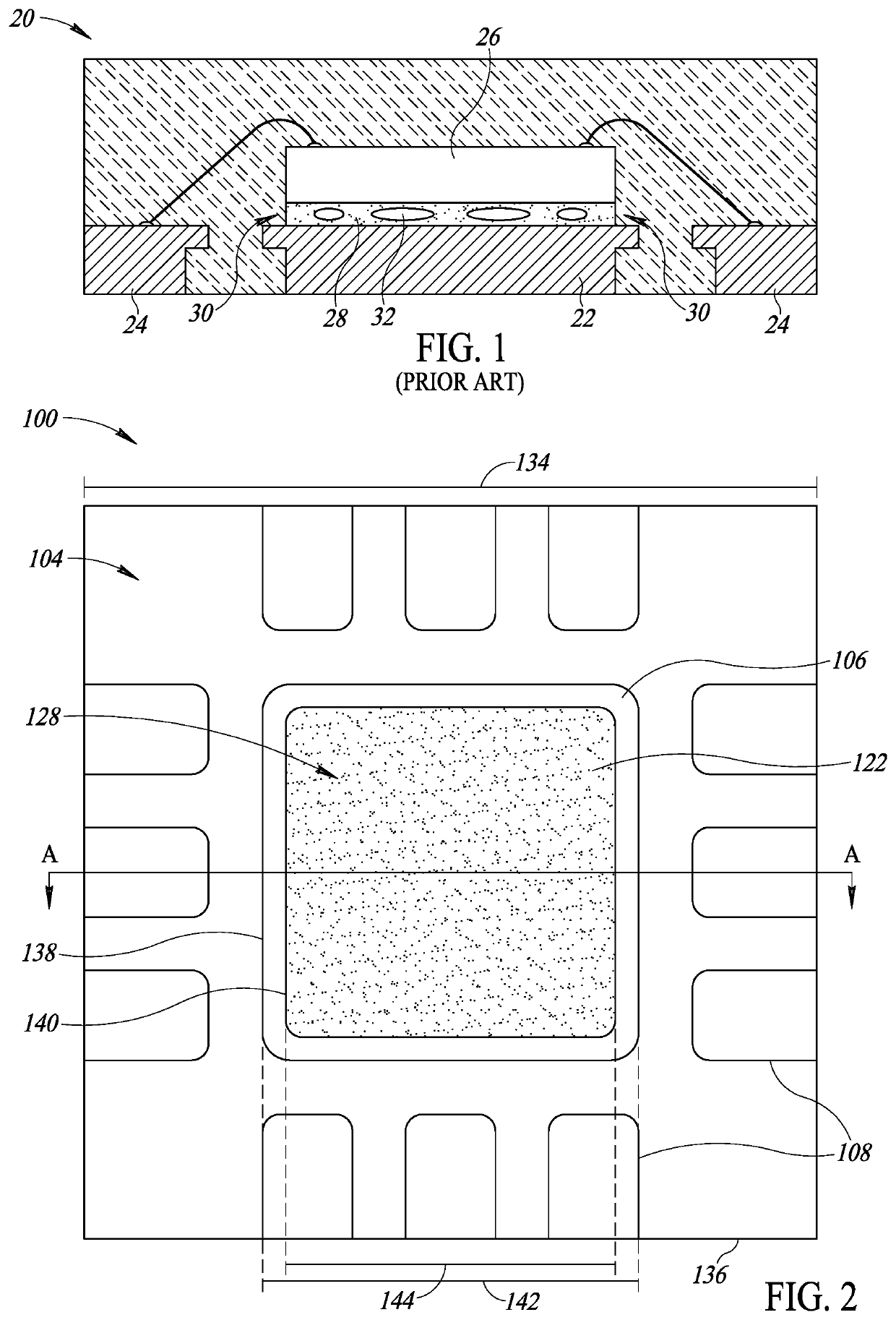
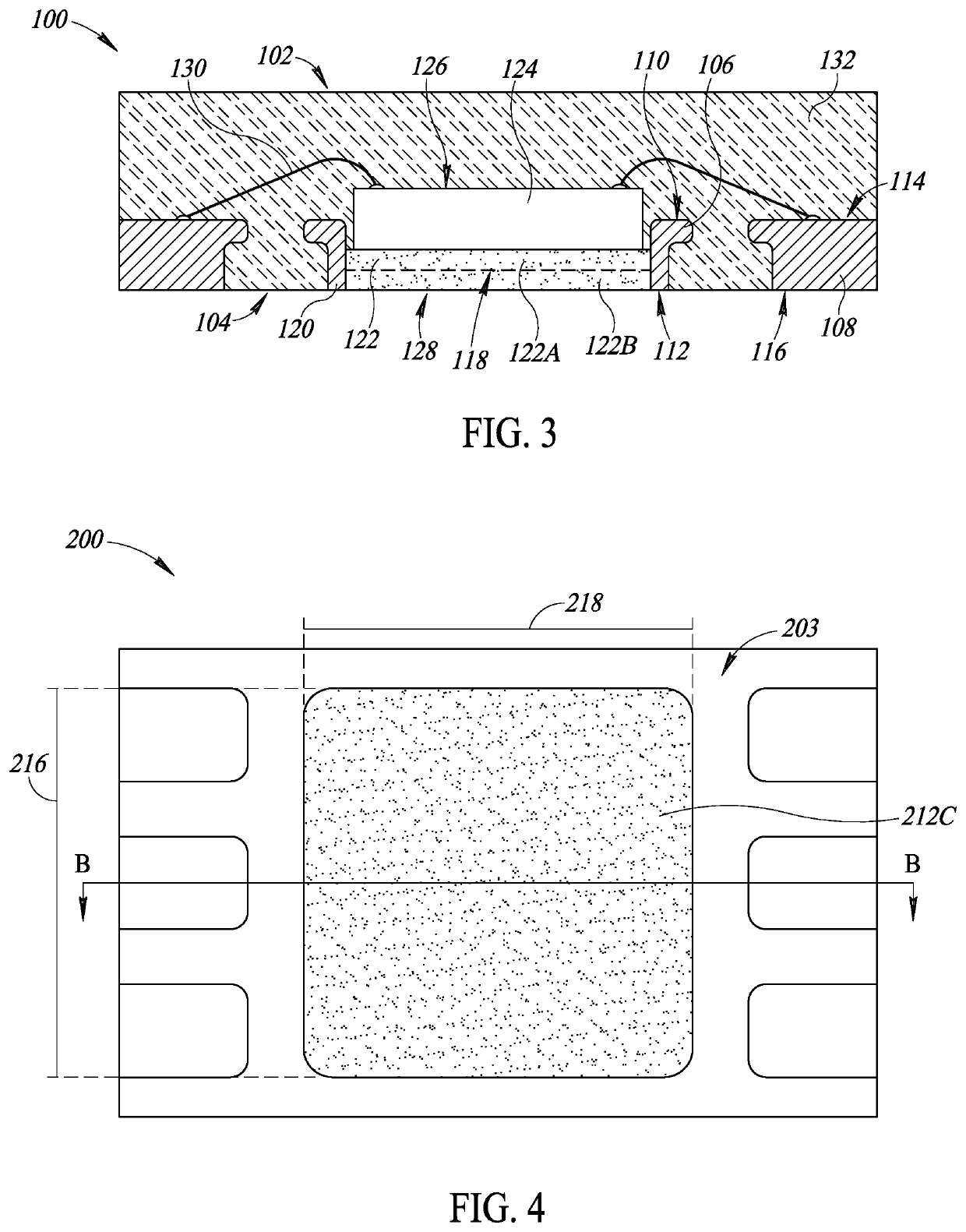
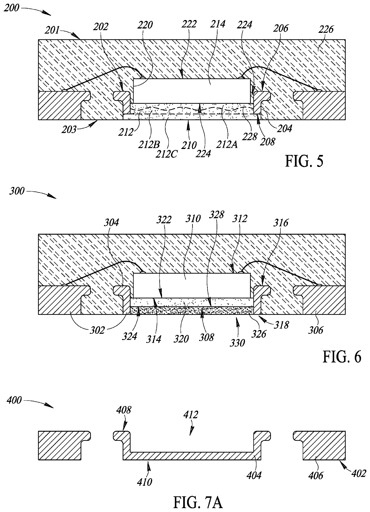
[0019]The present disclosure is generally directed to semiconductor packages having a cavity or aperture in a die pad of the package with solder or other material in the cavity coplanar with a surface of the die pad. The cavity allows for solder voids in the solder to escape during solder reflows, thus reducing the presence of solder voids and increasing thermal performance of the package.

[0020]FIG. 1 illustrates a known semiconductor package 20. The package 20 includes a die pad 22 and a plurality of leads 24. A semiconductor die 26 is coupled to the die pad 22 with a die attach material 28, which may be solder. Because the die pad 22 is typically a solid block of metal, the material 28 is only exposed to the ambient environment at sides 30 of the material 28. FIG. 1 illustrates the package 20 significantly enlarged for clarity. In actuality, a typical package 20 is on the order of a few millimeters in width, length, and thickness. As such, the area of die attach material 28 expose...


PUM


Abstract

A semiconductor package having an aperture in a die pad and solder in the aperture coplanar with a surface of the package is disclosed. The package includes a die pad, a plurality of leads, and a semiconductor die coupled to the die pad with a die attach material. A cavity or aperture is formed through the die pad to expose a portion of the die attach material. Multiple solder reflows are performed to reduce the presence of voids in the die attach material. In a first solder reflow, the voids of trapped gas that form when attaching the die to the die pad are released. Then, in a second solder reflow, solder is added to the aperture coplanar with a surface of the die pad. The additional solder can be the same material as the die attach material or a different material.

Description

BACKGROUNDTechnical Field[0001]The present disclosure is directed to semiconductor devices and more particularly, semiconductor packages.Description of the Related Art[0002]Quad-flat no-leads (“QFN”) semiconductor packages are known. Such packages physically and electrically connect integrated circuits to substrates, such as printed circuit boards. During operation, the integrated circuit produces heat, which is dissipated to avoid damage to the package. In known QFN packages, the heat produced by the integrated circuit is dissipated from the integrated circuit through the die pad to which the integrated circuit is coupled, and into the substrate or a thermal pad on the substrate. In attaching the integrated circuit to the die pad of the package, solder material is commonly used because of its high thermal conductivity. However, solder material has volatile components, such as flux, that create bubbles of gas that are trapped during solidification of the solder when coupling the int...

Claims


Application Information

Patent Timeline
IPC IPC(8): H01L23/495H01L23/31H01L21/48H01L21/56
CPCH01L21/565H01L23/49513H01L23/4952H01L21/4825H01L23/49548H01L23/3114H01L23/49503H01L23/3107H01L2224/73265H01L24/32H01L2224/32245H01L2224/48091H01L2224/48247H01L2924/181H01L2224/48464H01L2224/32105H01L2924/15153H01L2224/48476H01L2224/85801H01L2224/73267H01L24/82H01L2224/82002H01L2224/82101H01L2224/8284H01L2224/8285H01L2224/291H01L2224/29082H01L2224/83001H01L2224/83815H01L2224/83986H01L24/83H01L24/29H01L24/48H01L24/24H01L2224/24247H01L24/85H01L2224/451H01L2224/92247H01L2224/92244H01L2224/83385H01L24/92H01L24/73H01L24/45H01L2224/29111H01L2224/453H01L2224/4519H01L2224/29139H01L2224/29116H01L2224/29147H01L2924/3841H01L2924/35121H01L2924/00012H01L2924/00014H01L2924/014H01L2924/07811H01L2924/01082H01L2924/01029H01L2924/01047H01L2924/0105H01L24/30H01L24/49H01L24/33
Inventor TALLEDO, JEFFERSON
Owner STMICROELECTRONICS SRL
Why Eureka
Try Eureka