Multiple NANO layer transistor layers with different transistor architectures for improved circuit layout and performance

a technology of nano-layer transistors and transistor architectures, applied in the field of micro-electronic devices, can solve the problems of affecting the application of logic designs, scaling efforts are running into greater challenges,

Active Publication Date: 2020-12-31
TOKYO ELECTRON LTD
View PDF0 Cites 9 Cited by
  • Summary
  • Abstract
  • Description
  • Claims
  • Application Information

AI Technical Summary

Benefits of technology

[0005]Techniques herein include 3D architectures and methods of making 3D transistors using multiple selective nano-sheets for fabrication in different device regions (i.e. NMOS, PMOS, and new device types). By optimizing the layout of the nano-sheet planes, more efficient device layout is possible for building diff

Problems solved by technology

Scaling efforts have greatly increased the number of transistors per unit area in 2D circuits, yet scaling efforts are running into greater challenges as scaling enters single digit nanometer semiconductor device fabr

Method used


Image

  • Multiple NANO layer transistor layers with different transistor architectures for improved circuit layout and performance
  • Multiple NANO layer transistor layers with different transistor architectures for improved circuit layout and performance
  • Multiple NANO layer transistor layers with different transistor architectures for improved circuit layout and performance

Examples


Embodiment Construction

[0015]Reference throughout this specification to “one embodiment” or “an embodiment” means that a particular feature, structure, material, or characteristic described in connection with the embodiment is included in at least one embodiment of the application, but do not denote that they are present in every embodiment.

[0016]Thus, the appearances of the phrases “in one embodiment” or “in an embodiment” in various places throughout this specification are not necessarily referring to the same embodiment of the application. Furthermore, the particular features, structures, materials, or characteristics may be combined in any suitable manner in one or more embodiments.

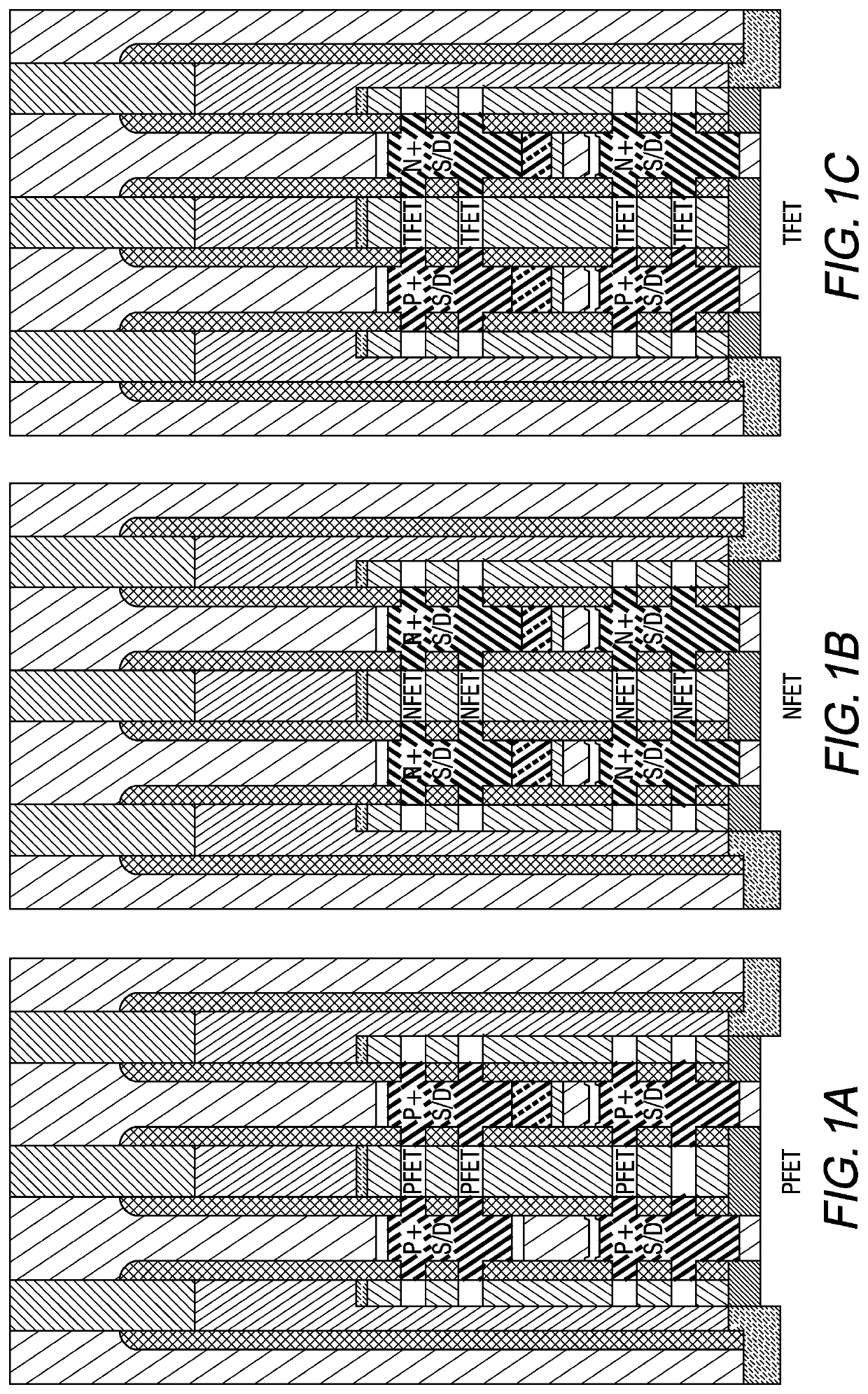
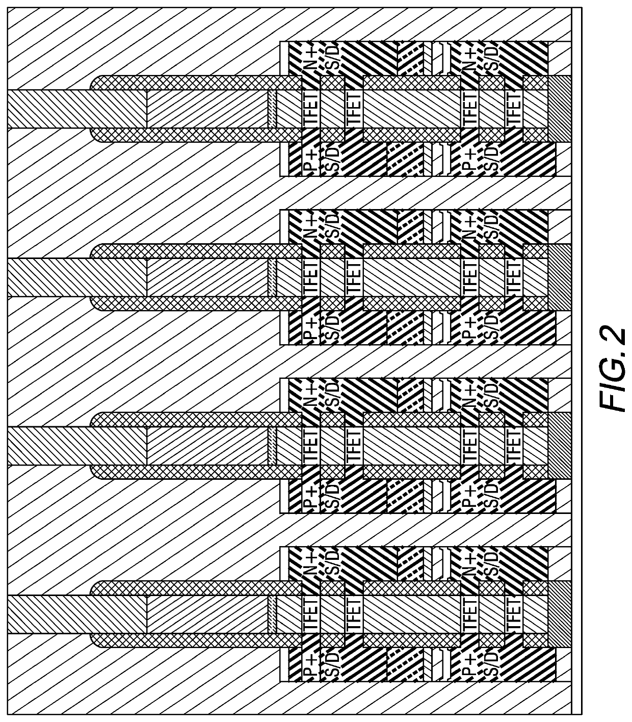
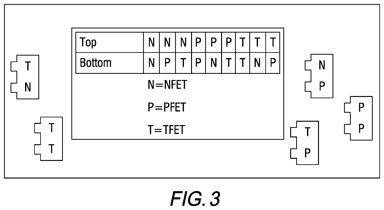
[0017]Devices herein are embodied using nano-wires or nano-sheets. The term “nano-channel” herein means either a nano-wire or a nano-sheet shaped channel for a field effect transistor. A nano-wire is a relatively small elongated structure formed having a generally circular cross section or rounded cross section. Nano-wires ...


PUM


Abstract

A semiconductor device includes a plurality of nano-channel field-effect transistor stacks positioned adjacent to each other such that source-drain regions are shared between adjacent nano-channel field-effect transistor stacks, each nano-channel field-effect transistor stack including at least two nano-channel field-effect transistors and corresponding source/drain regions vertically separated from each other.

Description

CROSS REFERENCE TO RELATED APPLICATIONS[0001]This application is based on and claims the benefit of and priority to U.S. Provisional Patent Application No. 62 / 866,975, entitled “MULTIPLE NANO LAYER TRANSISTOR LAYERS WITH DIFFERENT TRANSISTOR ARCHITECTURES FOR IMPROVED CIRCUIT LAYOUT AND PERFORMANCE”, filed on Jun. 26, 2019, the entire contents pf which are herein incorporated by reference.BACKGROUNDTechnical Field[0002]The present application relates to microelectronic devices, including semiconductor devices, transistors, and integrated circuits. More particularly, it relates to manufacturing of three-dimensional (3D) transistors, including combinations of various field-effect transistors (FETs).Description of the Related Art[0003]In the manufacture of a semiconductor device (especially on the microscopic scale), various fabrication processes are executed such as film-forming depositions, etch mask creation, patterning, material etching and removal, and doping treatments. These pro...

Claims


Application Information

Patent Timeline
IPC IPC(8): H01L27/092H01L27/088H01L21/8238H01L21/822
CPCH01L27/0924H01L21/823821H01L21/8221H01L21/823814H01L27/0886H01L29/42392H01L29/78696H01L27/0688H01L27/088H01L27/092H01L21/823425
Inventor FULFORD, H. JIMGARDNER, MARK I.
Owner TOKYO ELECTRON LTD
Why Eureka
Try Eureka