
Three dimensional resistive random access memory and method enabling such a memory to be obtained

a random access memory and three-dimensional technology, applied in the field of memory, can solve the problems of leakage paths and configuration has not yet been implemented, and achieve the effects of improving the performance of the memory device, increasing the storage density, and reducing manufacturing costs

Active Publication Date: 2020-12-31
COMMISSARIAT A LENERGIE ATOMIQUE ET AUX ENERGIES ALTERNATIVES
View PDF0 Cites 2 Cited by
  • Summary
  • Abstract
  • Description
  • Claims
  • Application Information

AI Technical Summary

Benefits of technology

The invention proposes a solution to problems in traditional 2D memories by providing a 3D memory device. This device uses a selector for each memory point, which helps to reduce leakage paths and improve performance. The geometry of the selectors can be controlled by modulating the thickness of the layer of active material and the distance between the flat electrode and the vertical electrode. This allows for the formation of a filament enabling the storage of information. The method also allows for selective etching of conductive materials and control of the geometry of the proximal end of the flat electrode and its associated selectors. These technical effects make the 3D memory device more efficient, cost-effective, and more suitable for high-density storage.

Problems solved by technology

In the technology of two dimensional (hereafter 2D) memories, a known problem linked to the addressing of a memory point PM is that of leakage paths.
However, such a configuration has not until now been put in place in the case of 3D memories.

Method used


Image

  • Three dimensional resistive random access memory and method enabling such a memory to be obtained
  • Three dimensional resistive random access memory and method enabling such a memory to be obtained
  • Three dimensional resistive random access memory and method enabling such a memory to be obtained

Examples


Embodiment Construction

[0093]Unless stated otherwise, a same element appearing in the different figures has a single reference.

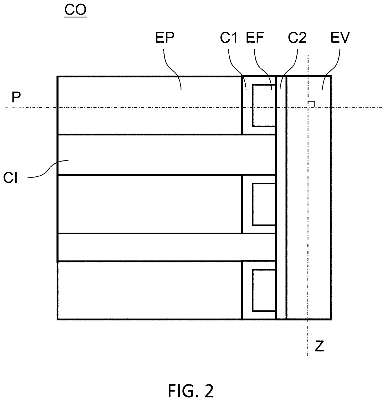
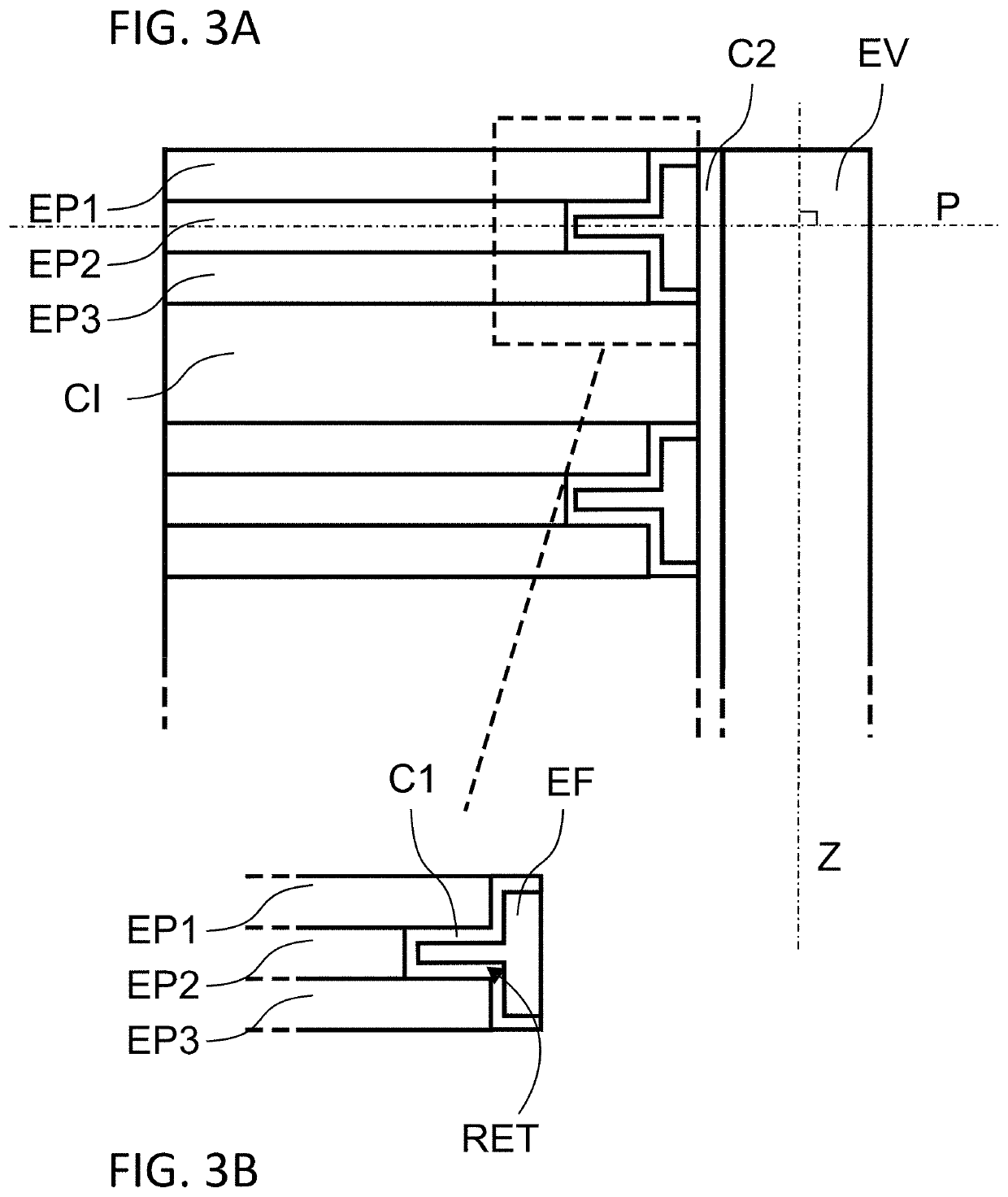
[0094]A first aspect of the invention illustrated in FIGS. 2 to 4 relates to a 3D memory CO comprising a plurality of memory points PM and a plurality of selectors, each memory point of the plurality of memory points being associated with a selector of the plurality of selectors. More particularly, in an embodiment, the 3D memory CO according to a first aspect of the invention comprises a plurality of first electrodes EP made of a conductive material, referred to as flat electrodes EP, each flat electrode EP of the plurality of flat electrodes EP defining a plane P. The memory also comprises a second electrode made of a conductive material, referred to as vertical electrode EV, extending essentially along an axis perpendicular to the plane defined by each flat electrode EP of the plurality of flat electrodes EP. The 3D memory according to a first aspect of the invention also compr...


PUM


Abstract

A three dimensional memory includes flat electrodes, each defining a plane; a vertical electrode, extending essentially along an axis perpendicular to the plane defined by each flat electrode; floating electrodes, each situated between a flat electrode and the vertical electrode; first layers of an insulating material, each flat electrode being separated from the preceding and / or following flat electrode by a first layer of an insulating material; first layers of a first active material, each layer of an active material separating a flat electrode from the floating electrode that is associated therewith; a second layer of a second active material separating the vertical electrode from the floating electrodes. The first active material forms a selector or a memory point and the second active material forms a memory point or a selector. Each flat electrode includes first, second and third sub-layers made of, respectively, first, second and third conductive materials.

Description

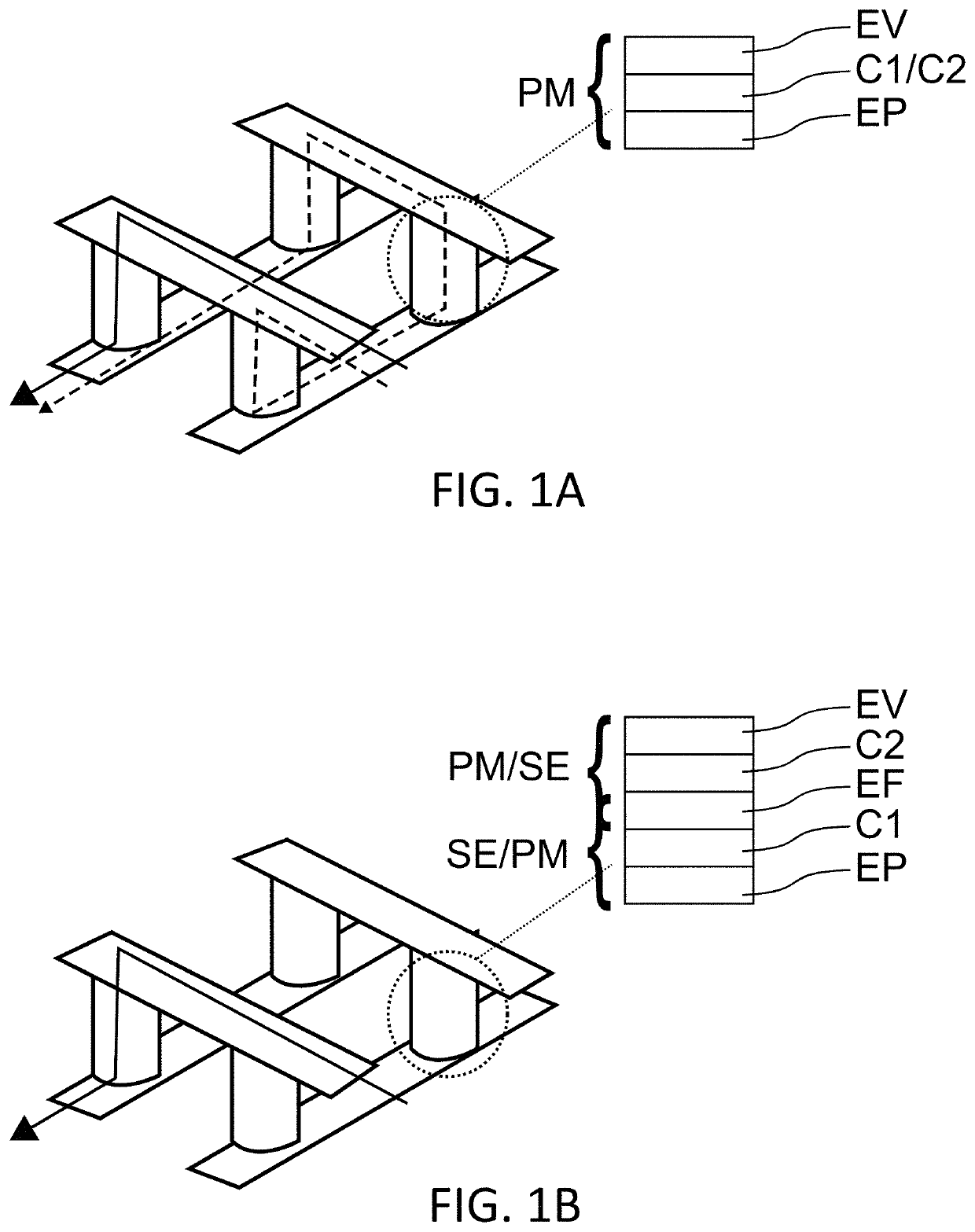
TECHNICAL FIELD OF THE INVENTION[0001]The technical field of the invention is that of memories. The present invention relates to a three dimensional (hereafter 3D) memory and in particular a 3D memory wherein a selector is associated with each memory point. The invention also relates to a method enabling such a memory to be obtained.TECHNOLOGICAL BACKGROUND OF THE INVENTION[0002]In the technology of two dimensional (hereafter 2D) memories, a known problem linked to the addressing of a memory point PM is that of leakage paths. Indeed, as illustrated in FIG. 1A, when a reading potential is applied to a line and to a column in order to read a memory point PM of an array of memory points PM, the current passes not only through the target memory point PM (that is to say situated at the intersection of the selected line and column—solid line arrow), but also by parasitic paths (dashed line arrows) which may alter the reading of the memory point PM.[0003]In 2D structures, it is easy to red...

Claims


Application Information

Patent Timeline
IPC IPC(8): H01L27/24H01L45/00
CPCH01L27/2409H01L45/1675H01L45/1226H01L27/249H01L45/1253G11C2213/71G11C2213/52G11C2213/76G11C13/003G11C13/0004G11C13/0007H10B63/20H10B63/845H10N70/231H10N70/20H10N70/823H10N70/8828H10N70/8833H10N70/063H10N70/841
Inventor EL HAJJAM, KHALILMOLAS, GABRIELNODIN, JEAN-FRANÇOIS
Owner COMMISSARIAT A LENERGIE ATOMIQUE ET AUX ENERGIES ALTERNATIVES
Learn More