Bidirectional Phase Controlled Thyristor (BiPCT) - A New Semiconductor Device Concept

a phase control, bidirectional technology, applied in the direction of semiconductor devices, basic electric elements, electrical equipment, etc., can solve the problems of high loss, thermal management, and inefficient use of semiconductor wafers in the known five-layer switch-type device, so as to improve the turn-off capability of the bidirectional thyristor device, improve the thermal management of the device, and simplify the device manufacturing process

Active Publication Date: 2020-12-31
HITACHI ENERGY SWITZERLAND AG
View PDF0 Cites 0 Cited by
  • Summary
  • Abstract
  • Description
  • Claims
  • Application Information

AI Technical Summary

Benefits of technology

[0020]In an exemplary embodiment, in the orthogonal projection onto the plane parallel to the first main side, at least the first gate electrode or the second gate electrode has a rotational symmetry. Such shape of the gate electrode with rotational symmetry allows most efficient use of the wafer area of thyristors for ceramic hockey-puck packages and improves thermal management of the device.
[0021]In an exemplary embodiment, when being viewed in the orthogonal projection onto the plane parallel to the first main side, the first gate electrode and the second gate electrode have the same shape. Such same shape of the first and second gate electrode allows to simplify the process of manufacturing the device as the same mask designs can be used for structuring the first and second gate electrodes.
[0022]In an exemplary embodiment a density of deep levels acting as recombination centers in the third semiconductor layer has a first local maximum which is closer to the second p-n junction than to the third p-n junction and / or a second local maximum which is closer to the third p-n junction than to the second p-n junction. The first local maximum may exemplarily be less than 50 μm from the second p-n junction, and / or the second local maximum may be exemplarily less than 50 μm from the third p-n junction. The local maximum of the density of deep levels acting as recombination centers in the third semiconductor layer close to the second and / or third p-n junction can improve the turn-off capability of the bidirectional thyristor device by commutation of anode voltage.
[0023]In an exemplary embodiment, an excess carrier lifetime has a first local minimum which is closer to the second p-n junction than to the third p-n junction and / or a second local minimum at a position which is closer to the third p-n junction than to the second p-n junction. The first local minimum may exemplarily be less than 50 μm from the second p-n junction, and / or the second local minimum may exemplarily be less than 50 μm from the third p-n junction. The local minimum of the excess carrier lifetime in the third semiconductor layer close to the second and / or third p-n junction can improve the turn-off capability of the bidirectional thyristor device by commutation of anode voltage.

Problems solved by technology

A configuration with two RC thyristors in back-to-back configuration has the disadvantage of high losses as the losses of the two thyristors add up in the serial connection.
However, of the two thyristor structures use different areas of a semiconductor wafer so that the area of the semiconductor wafer is not efficiently used in this known five-layer switch-type device.
A major challenge in the integration of the two thyristor halves in the BCT is to avoid cross talk between the two thyristor halves, which are separated from each other by a separation region in the semiconductor wafer.
Another problem in BCT device operation is the thermal management as heat generation is not homogeneously distributed over the whole wafer area.

Method used


Image

  • Bidirectional Phase Controlled Thyristor (BiPCT) - A New Semiconductor Device Concept
  • Bidirectional Phase Controlled Thyristor (BiPCT) - A New Semiconductor Device Concept
  • Bidirectional Phase Controlled Thyristor (BiPCT) - A New Semiconductor Device Concept

Examples


Embodiment Construction

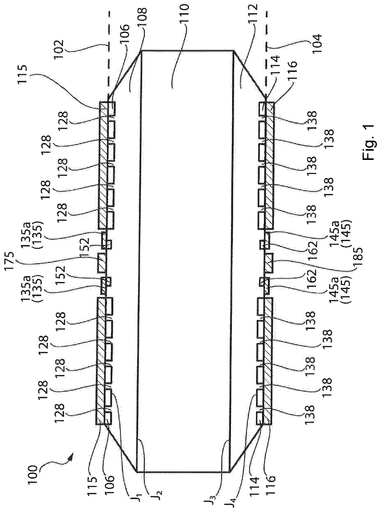
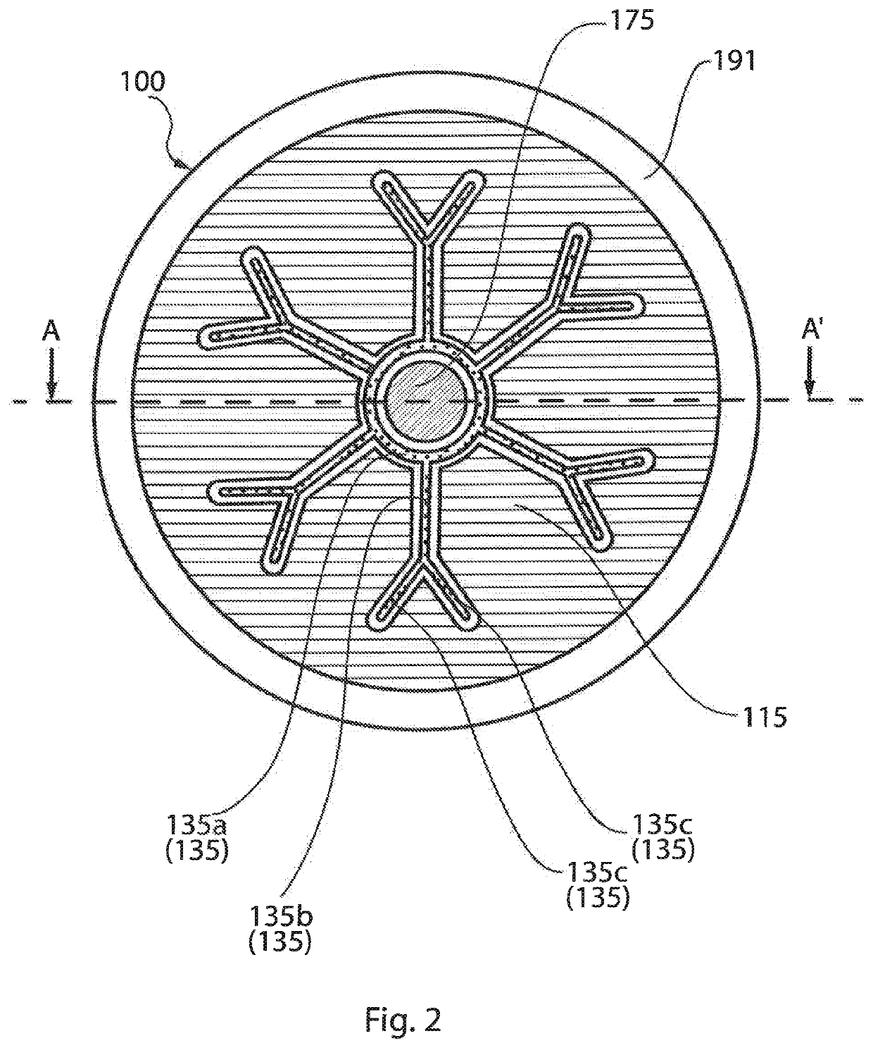
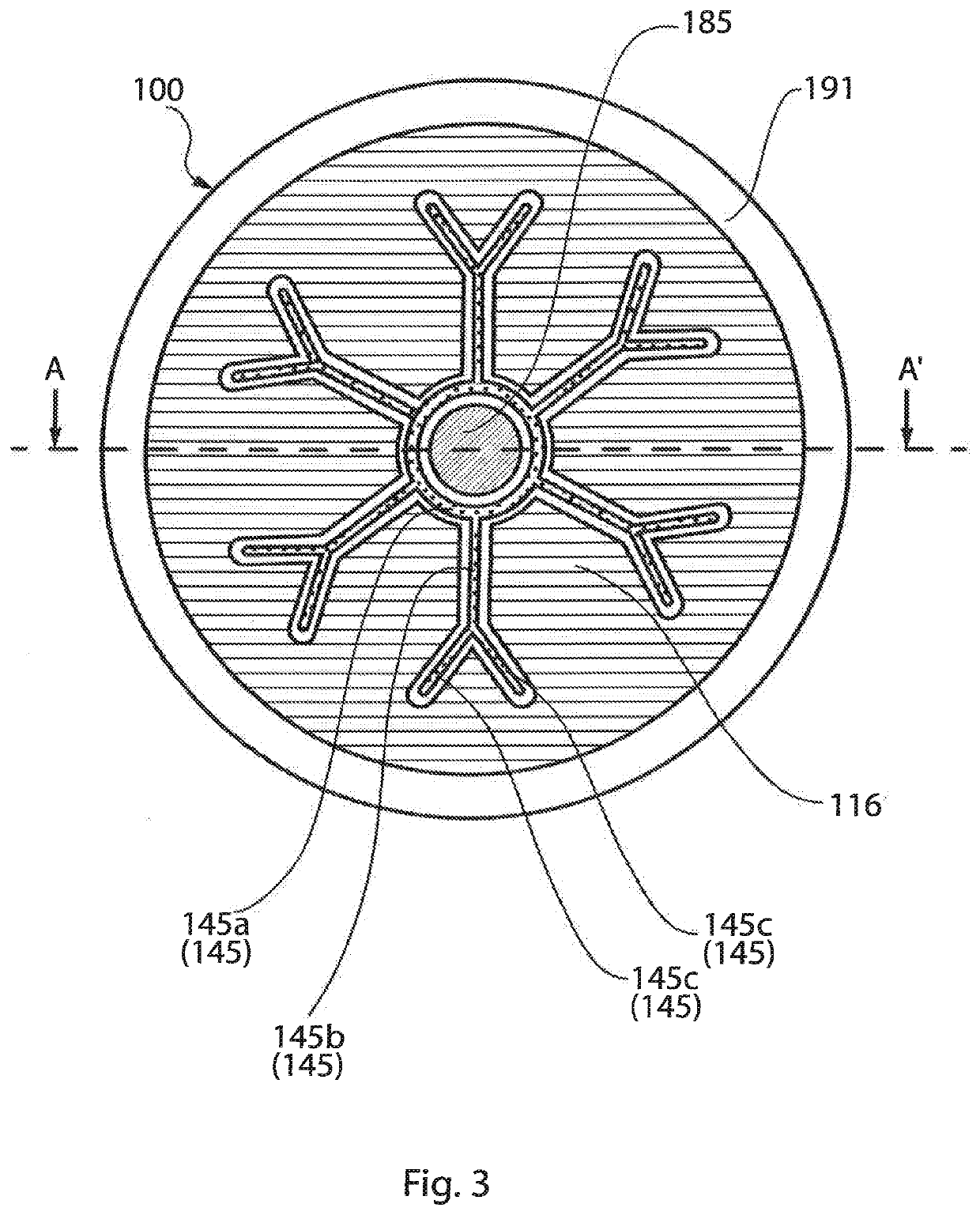
[0033]FIG. 1 shows a vertical cross-section of a bidirectional thyristor device 100 according to an embodiment of the invention, FIG. 2 shows a top view of the bidirectional thyristor device 100 and FIG. 3 shows a bottom view of the bidirectional thyristor device 100. The bidirectional thyristor device 100 comprises a semiconductor wafer having a first main side 102 and a second main side 104 opposite and parallel to the first main side 102. The plane of the drawing in FIG. 1 is a plane perpendicular to the first main side 102. The cross-section shown in FIG. 1 is taken along a line A-A′ in FIGS. 2 and 3, respectively.

[0034]In an order from the first main side 102 of the semiconductor wafer, the semiconductor wafer comprises an n+-doped first semiconductor layer 106, a p-doped second semiconductor layer 108, an n−-doped third semiconductor layer 110, a p-doped fourth semiconductor layer 112, and an n+-doped fifth semiconductor layer 114. The n+-doped first semiconductor layer 106 an...


PUM

PropertyMeasurementUnit
lateral sizeaaaaaaaaaa
rating currentaaaaaaaaaa

Abstract

A bidirectional thyristor device includes a semiconductor wafer with a number of layers forming pn junctions. A first main electrode and a first gate electrode are arranged on a first main side of the wafer. A second main electrode and a second gate electrode are arranged on a second main side of the wafer. First emitter shorts penetrate through a first semiconductor layer and second emitter shorts penetrate through a fifth semiconductor layer. In an orthogonal projection onto a plane parallel to the first main side, a first area occupied by the first semiconductor layer and the first emitter shorts overlaps in an overlapping area with a second area occupied by the fifth semiconductor layer and the second emitter shorts. The overlapping area, in which the first area overlaps with the second area, encompasses at least 50% of a total wafer area occupied by the semiconductor wafer.

Description

FIELD OF THE INVENTION[0001]The present invention relates to a bidirectional thyristor device implemented in a single semiconductor wafer.BACKGROUND OF THE INVENTION[0002]A thyristor, sometimes also referred to as silicon controlled rectifier (SCR), is a switching semiconductor device which can be turned on in a forward direction, i.e. when being forward biased, by supplying a positive gate trigger current pulse to a gate terminal. The thyristor is then said to be in a forward conducting state or on-state in which a current can flow in a forward direction from an anode to a cathode. On the other hand, the thyristor can also be in a forward blocking state, also referred to as off-state, meaning that the flow of a high current through anode can be blocked and a thyristor withstands a high positive voltage in the forward direction. In a reverse direction opposite to the forward direction, the thyristor cannot be turned on. A thyristor may be reverse blocking, which means that it can ma...

Claims


Application Information

Patent Timeline
Patent Type & Authority Applications(United States)
IPC IPC(8): H01L29/747H01L29/06H01L29/08H01L29/423
CPCH01L29/42308H01L29/0692H01L29/747H01L29/0839H01L29/0834H01L29/7404
Inventor VOBECKY, JANVEMULAPATI, UMAMAHESWARARAHIMO, MUNAF
Owner HITACHI ENERGY SWITZERLAND AG
Why Eureka
Try Eureka