OLED display device and method for manufacturing same

a technology of light-emitting diodes and display devices, which is applied in the field of display technology, can solve the problems of loss of over 55% of light emitted from display panels, inability to use dynamically bendable display products, and easy breakage of polarizers, etc., and achieve excellent flexibility and bending characteristics, reduce thickness of oled display devices, and increase the light transmittance of oled devices

Active Publication Date: 2021-01-21
WUHAN CHINA STAR OPTOELECTRONICS SEMICON DISPLAY TECH CO LTD
View PDF0 Cites 3 Cited by
  • Summary
  • Abstract
  • Description
  • Claims
  • Application Information

AI Technical Summary

Benefits of technology

[0042]Compared to prior art, the present disclosure provides an organic light emitting diode (OLED) display device and a method for manufacturing the same. By embedding the color filter layer in the thin film encapsulation layer, a thickness of the OLED display device is reduced. This makes the OLED display device have more excellent flexibility and bending characteristics, and increases light transmittance of the OLED devices. In addition, the processes for forming the color filter layer and the thin film encapsulation layer are compatible with each other. It is easy to form the color filter layer of the present disclosure, thus shortening the manufacturing process of display devices and lowering the manufacturing costs of display devices without resulting in defects in products. Further, by forming a low light reflection film on top surface of the metal layer of the touch sensor, the light reflection problems of display devices existing in prior art are solved.

Problems solved by technology

However, the polarizer results in loss of over 55% of light emitted from the display panels.
Moreover, polarizer is primarily made of polyvinyl alcohol (PVA), which is thick in thickness (about 100 μm) and is fragile, and thus it is likely that a polarizer is easily broken if it is bent, and cannot be used for dynamically bendable display products.
During a patterning process of the color filter layer, alkaline development liquid enters the thin film encapsulation layer, and affects OLED devices, resulting in defects in products and lowering manufacturing yield of products.
The patterning process is complicated.
This makes the display devices to have a long time manufacturing process, and increases manufacturing costs.
Moreover, although use of the POL-less technique can mitigate light reflection issues, electrodes of touch sensors, which are made of metal, still cause light reflection in OLED display devices.
The POL-less technique cannot completely solve the light reflection issues.

Method used


Image

  • OLED display device and method for manufacturing same
  • OLED display device and method for manufacturing same
  • OLED display device and method for manufacturing same

Examples


Embodiment Construction

[0044]The following embodiments refer to the accompanying drawings for exemplifying specific implementable embodiments of the present disclosure. Moreover, directional terms described by the present disclosure, such as upper, lower, front, back, left, right, inner, outer, side, etc., are only directions by referring to the accompanying drawings, and thus the used directional terms are used to describe and understand the present disclosure, but the present disclosure is not limited thereto. In the drawings, the same reference symbol represents the same or similar components.

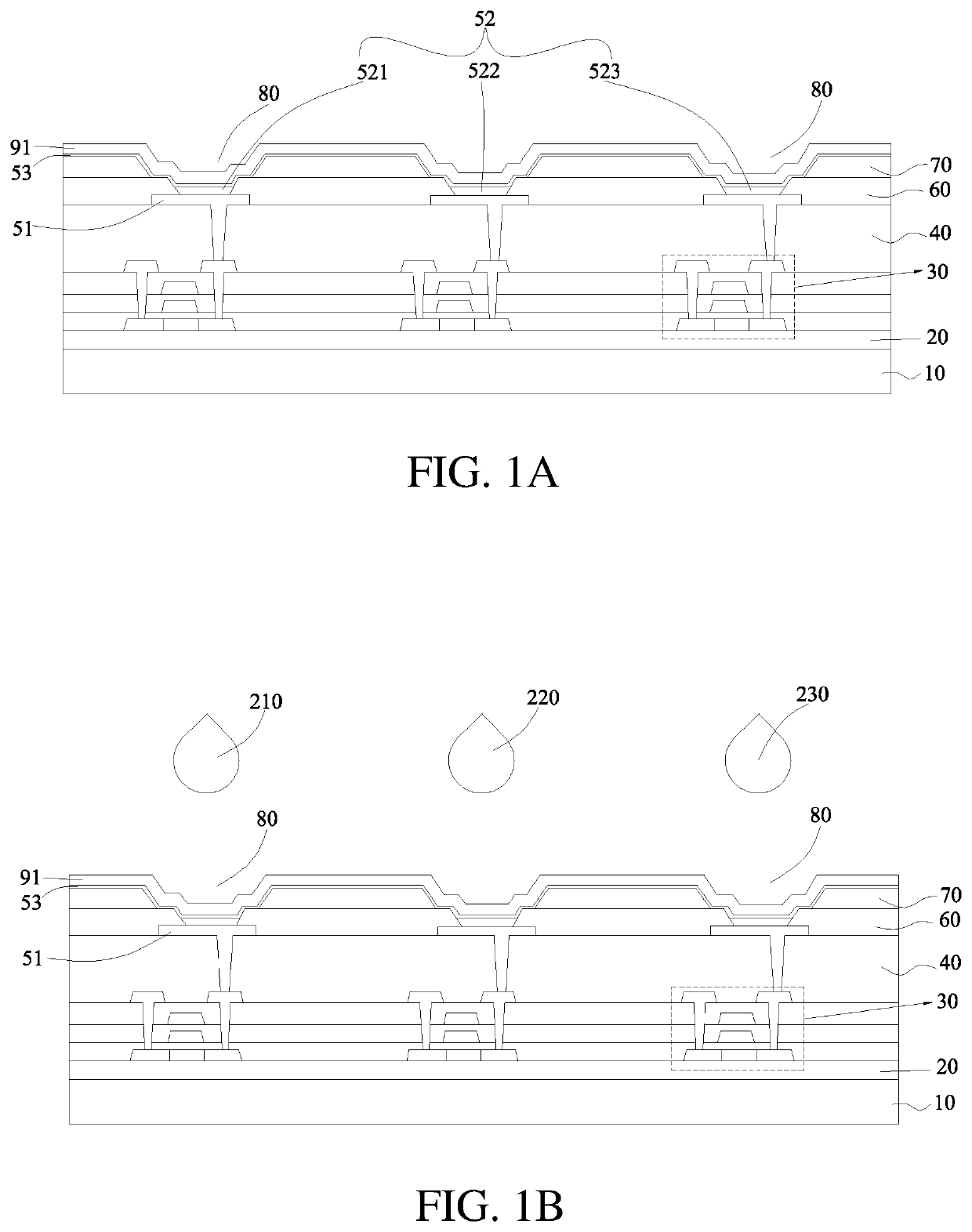
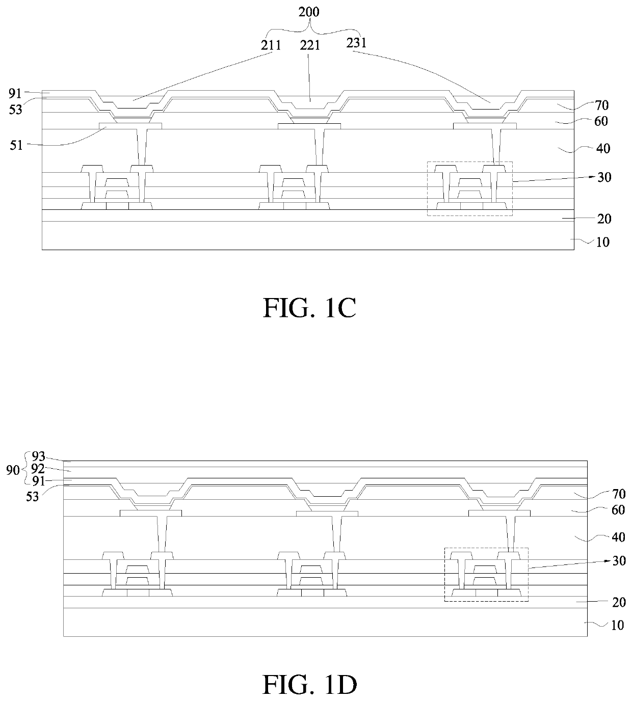
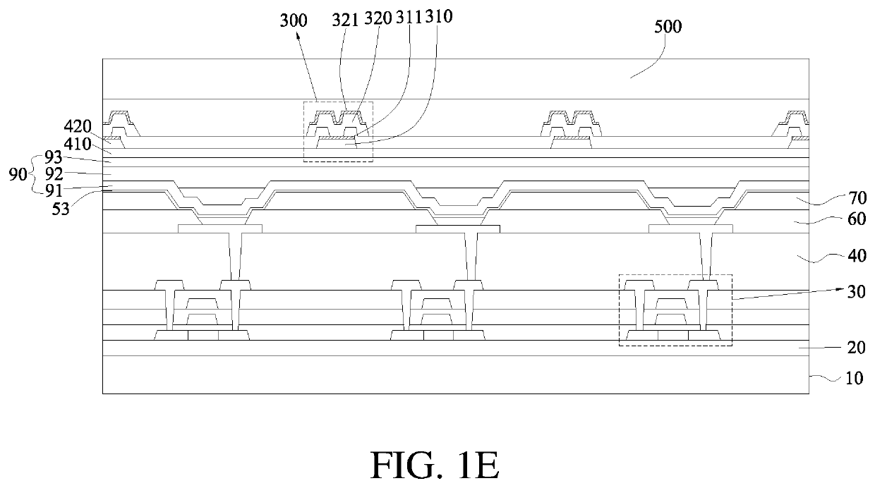
[0045]Please refer to FIGS. 1A to 1E, which show each step in a process flow of a method for manufacturing an organic light emitting diode (OLED) display device according to the present disclosure. The present disclosure provides the method for manufacturing the organic light emitting diode (OLED) display device. The method includes formation of a display panel and a touch panel. The method includes a lot of steps...


PUM

PropertyMeasurementUnit
thicknessaaaaaaaaaa
reflectivityaaaaaaaaaa
temperatureaaaaaaaaaa

Abstract

The present disclosure provides an organic light emitting diode (OLED) display device and a method for manufacturing the same. The OLED display device includes a substrate; a pixel defining layer disposed on the substrate and defining an opening; a first thin film encapsulation sublayer disposed on the pixel defining layer and in the opening; a color filter layer disposed in the opening; a second thin film encapsulation sublayer covering the first thin film encapsulation sublayer and the color filter layer; and a third thin film encapsulation sublayer disposed on the second thin film encapsulation sublayer.

Description

FIELD OF INVENTION[0001]The present disclosure relates to a field of display technology, and more particularly, to an organic light emitting diode (OLED) display device and a method for manufacturing the same.BACKGROUND[0002]Because organic light emitting diode (OLED) display devices have advantages, such as light weight, thin thickness, self-illumination, short response times, wide viewing angles, wide color gamut, high brightness, and low power consumption among various types of display techniques, OLED display devices have attracted user attention in recent years.[0003]To solve low contrast issues of OLED display devices due to a strong outdoor light environment, a polarizer is generally disposed on OLED display panels. However, the polarizer results in loss of over 55% of light emitted from the display panels. Moreover, polarizer is primarily made of polyvinyl alcohol (PVA), which is thick in thickness (about 100 μm) and is fragile, and thus it is likely that a polarizer is easi...

Claims


Application Information

Patent Timeline
Patent Type & Authority Applications(United States)
IPC IPC(8): H01L27/32H01L51/52G06F3/041
CPCH01L27/322H01L27/323H01L27/3246H01L51/0097H01L51/5284G06F3/0412H01L51/5253H10K59/50H10K59/40H10K50/856H10K59/1201H10K71/00G06F2203/04103H10K59/38H10K50/844H10K50/86H10K2102/311H10K50/865H10K59/122H10K77/111
Inventor XIANYU, WENXUGONG, WENLIANG
Owner WUHAN CHINA STAR OPTOELECTRONICS SEMICON DISPLAY TECH CO LTD
Why Eureka
Try Eureka