Optical device, imaging device, focus driving method, and method for moving lens center

Active Publication Date: 2021-02-11
UNIV OF ELECTRONIC SCI & TECH OF CHINA
View PDF0 Cites 0 Cited by
  • Summary
  • Abstract
  • Description
  • Claims
  • Application Information

AI Technical Summary

Benefits of technology

This patent text describes an optical device with a special spatial distribution of electric field that is controlled by the uniformity of impedance membrane. The device has a light transmission hole with a parallelogram shape that allows for a stable focus and efficient utilization of optical energy. The technical effects of this design include improved focal distance adjustment and stability, as well as higher utilization rate of optical energy.

Problems solved by technology

However, a typical liquid crystal lens has a relatively-small light transmission hole, which limits the application of the liquid crystal lens in the imaging area.
However, this type of structure caused the problem of an increased driving voltage.
However, the instability of the high impedance membrane is still unsolved, which is mainly reflected in: at present, the high impedance membrane is mainly made of metal oxides and conductive organic polymers; as the conditions or environments of later processes change, electrical properties of the high impedance membrane change, which further affects the imaging effect of the liquid crystal lens; secondly, electrical properties of the performance of the high impedance membrane changes with time and environmental conditions, resulting in a poor stability of the liquid crystal lens.
However, due to the limitation of the production process, it is difficult to produce the impedance membrane with the specified impedance, thus the cost of preparing the liquid crystal optical device according to the technical solution is relatively high.
At the same time, even if the high impedance membrane has a stable boundary value, the impedance of the high impedance membrane may change with time in the usage, and the change of the impedance of the high impedance membrane will lead to the uncertainty of focal length adjustment.

Method used


Image

  • Optical device, imaging device, focus driving method, and method for moving lens center
  • Optical device, imaging device, focus driving method, and method for moving lens center
  • Optical device, imaging device, focus driving method, and method for moving lens center

Examples


first embodiment

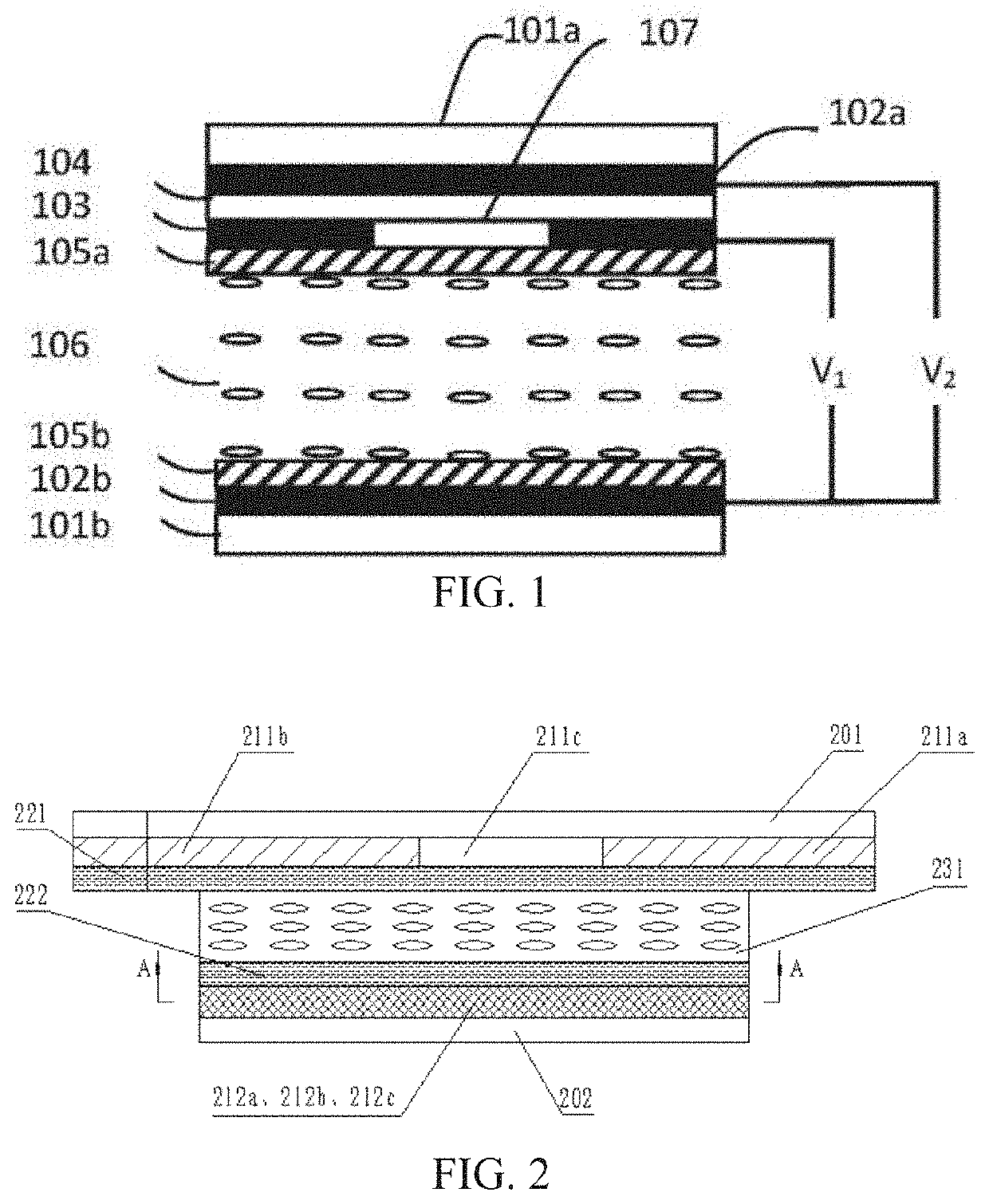
[0089]As shown from FIG. 2 to FIG. 5, an optical device in accordance with the first embodiment of the present invention includes a first substrate, a first electrode layer, a first alignment layer, a liquid crystal layer, a second alignment layer, a second electrode layer, and a second substrate arranged in turn along a light transmission direction. The first substrate and the second substrate are made of transparent glass. The first alignment layer and the second alignment layer are made of organic polymer or polystyrene, polyvinyl alcohol, epoxy resin or polyimide. An alignment direction of the first alignment layer is anti-parallel with that of the second alignment layer.

[0090]The first electrode layer includes a first electrode, a second electrode, and a first impedance membrane arranged between the first electrode and the second electrode. The first electrode and the second electrode are respectively arranged on a left end and a right end of the first impedance membrane. The s...

example 1

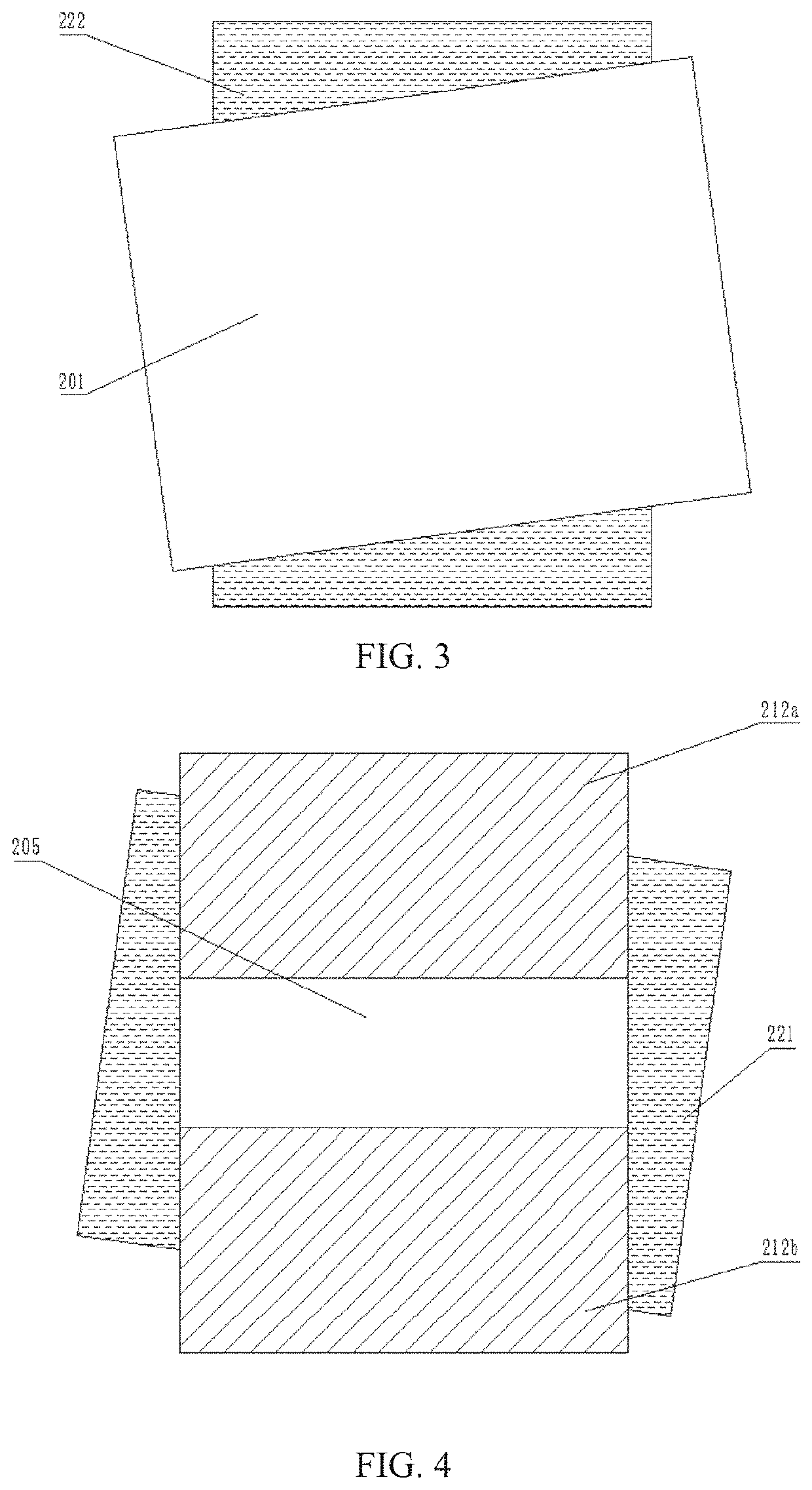
[0105]As shown from FIG. 14 to FIG. 16, in example 1, an optical device includes a first substrate, a first electrode layer, a second substrate, a first alignment layer, a liquid crystal layer, a second electrode layer, and a second substrate arranged in turn from top to bottom. A rubbing direction of the first alignment layer is anti-parallel with that of the second alignment layer. Projections of the first substrate, the first electrode layer, the first alignment layer, the liquid crystal layer, the second alignment layer, the second electrode layer, and the second substrate along a light transmission direction are squares of same sizes.

[0106]The first electrode layer includes a first electrode, a first impedance membrane, and a second electrode. The first electrode and the second electrode are respectively arranged on a left side and a right side of the first impedance membrane. The left side of the first impedance membrane is connected to the first electrode and the right side o...

example 2

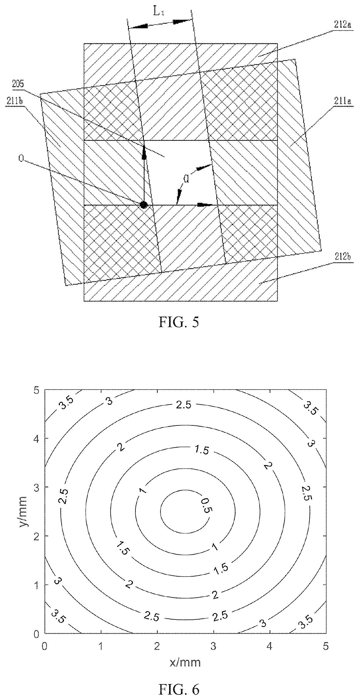
[0108]As shown from FIG. 18 to FIG. 20, an optical device of example 2 includes a first substrate, a first electrode layer, a first alignment layer, a liquid crystal layer, a second alignment layer, a second electrode layer, and a second substrate arranged in turn from top to bottom. A rubbing direction of the first alignment layer is anti-parallel with that of the second alignment layer.

[0109]The first electrode layer includes a first electrode, a first impedance membrane, and a second electrode. The first electrode and the second electrode are respectively arranged on a left side and a right side of the first impedance membrane. The left side of the first impedance membrane is connected to the first electrode and the right side of the first impedance membrane is connected to the second electrode. The second electrode layer includes a third electrode, a second impedance membrane, and a fourth electrode. The third electrode and the fourth electrode are respectively arranged on a fro...


PUM


Abstract

An optical device includes a first electrode layer, a first alignment layer, a liquid crystal layer, a second alignment layer, and a second electrode layer being arranged in turn along a light transmission direction; wherein the first electrode layer comprises a first electrode, a second electrode, and a first impedance membrane arranged between the first electrode and the second electrode, and the first electrode and the second electrode are respectively arranged on opposite ends of the first impedance membrane; the second electrode layer has a structure similar to that of the first electrode layer. The four electrodes form a light transmission hole being shaped as a parallelogram. The present invention solves the problem that the focal length of the liquid crystal lens cannot be accurately adjusted due to the instability of the impedance of the impedance membrane of the present liquid crystal lens.

Description

CROSS REFERENCE OF RELATED APPLICATION[0001]The present invention claims priority under 35 U.S.C. 119(a-d) to CN 201910735953.5, filed Aug. 9, 2019.BACKGROUND OF THE PRESENT INVENTIONField of Invention[0002]The present invention generally relates to optical devices, and more particularly, to an optical device, an imaging device, a focus driving method, and a method for moving a lens center.Description of Related Arts[0003]A liquid crystal lens is an optical device having a focal length which can be changed when an arrangement of liquid crystal molecules is changed by controlling a driving voltage. Liquid crystal molecules have dielectric anisotropy and birefringence effect, in an external electric field, a director orientation of the liquid crystal molecule changes as the electric field changes, and an effective refractive index in the corresponding direction correspondingly changes, thus, the liquid crystal lens can realize the function of convergence and divergence like traditiona...

Claims


Application Information

Patent Timeline
IPC IPC(8): G02F1/29
CPCG02F1/29G02F2001/294G02F2201/122G02F1/134309G02F1/13306G02F1/294
Inventor YE, MAOCHEN, XIAOXILI, GUANGYONGZHANG, YALEI
Owner UNIV OF ELECTRONIC SCI & TECH OF CHINA
Why Eureka
Try Eureka