Semiconductor Mach-Zehnder Modulator
a technology of optical modulator and semiconductor, applied in non-linear optics, instruments, optics, etc., can solve the problems of difficult to be them closely, large crosstalk between two i/q modulators, etc., and achieve stable differential transmission characteristic, small and low cost, and high bandwidth
- Summary
- Abstract
- Description
- Claims
- Application Information
AI Technical Summary
Benefits of technology
Problems solved by technology
Method used
Image

Examples
embodiment 1
Illustrative Embodiment 1
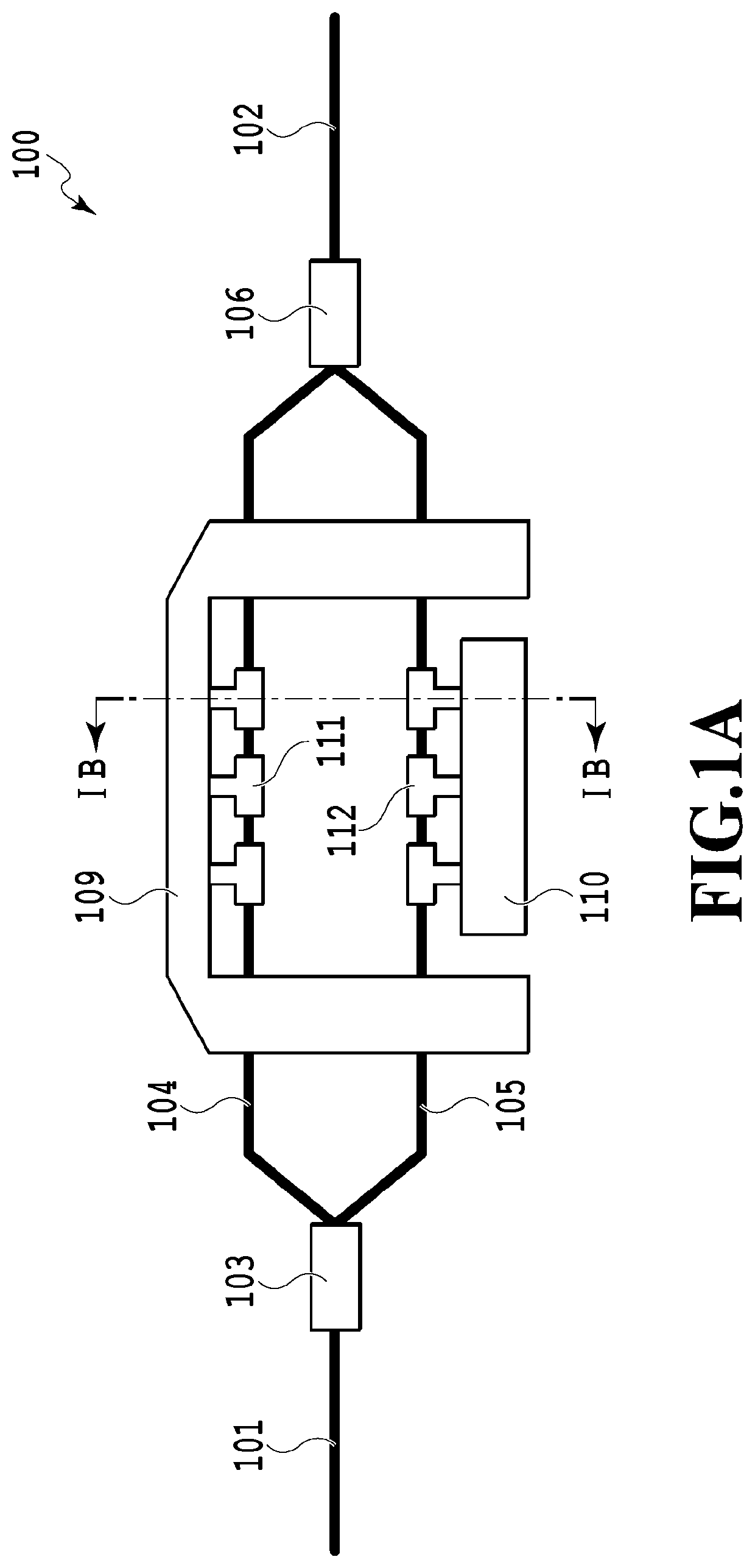
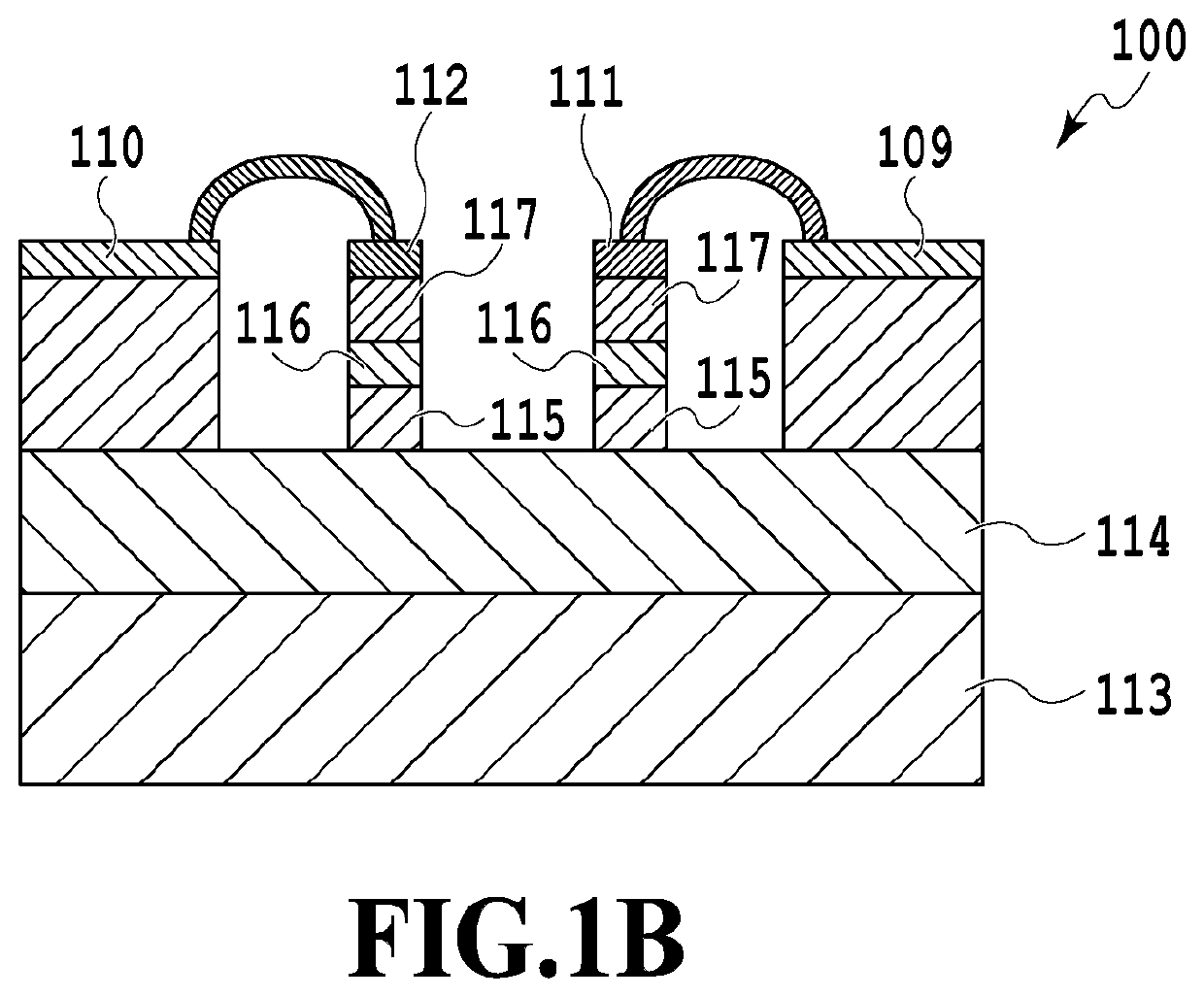
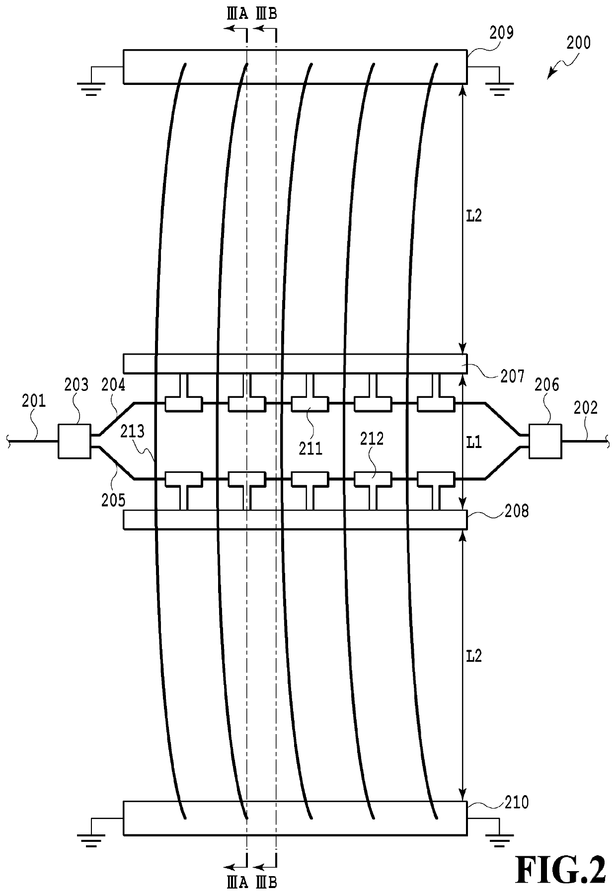
[0037]FIG. 2 illustrates the configuration of a semiconductor MZM 200 according to Illustrative Embodiment 1 of the present invention. FIG. 2 shows the semiconductor MZM 200 comprising: an input waveguide 201; an output waveguide 202; an optical demultiplexer 203 for demultiplexing a light wave wave-guided through the input waveguide 201 to two light waves; first and second arm waveguides 204 and 205 for wave-guiding the two demultiplexed light waves obtained through the optical demultiplexer 203, respectively; an optical demultiplexer 206 for demultiplexing the light waves wave-guided through the first and second arm waveguides 204 and 205, respectively, to output the resultant light waves to the output waveguide 202; a first signal electrode 207 formed in parallel with the first arm waveguide 204; a second signal electrode 208 formed in parallel with the second arm waveguide 205; a first ground electrode 209 parallelly formed along the first signal electro...
embodiment 2
Illustrative Embodiment 2
[0059]FIG. 6A illustrates the configuration of a semiconductor MZM 400 according to Illustrative Embodiment 2 of the present invention. FIG. 6B illustrates an example of the semiconductor MZM 400 according to Illustrative Embodiment 2 of the present invention taken along VIB. As shown in FIG. 6A and FIG. 6B, the semiconductor MZM 400 according to Illustrative Embodiment 2 of the present invention is configured so that the lower faces of the first and second ground electrodes 209 and 210 have thereon a plurality of the first and second vias 4011 and 4012. The back face of the SI—InP substrate 301 has thereon a plurality of back face ground electrodes 402 for connecting the first and second via 4011 and 4012. For example, the first and second ground electrodes 209 and 210 are connected by the plurality of back face ground electrodes 402 via a plurality of the first and second vias 4011 and 4012. The semiconductor MZM 400 according to Illustrative Embodiment 2 ...
embodiment 3
Illustrative Embodiment 3
[0063]FIG. 7A illustrates the configuration of a semiconductor MZM 500 according to Illustrative Embodiment 3 of the present invention. FIG. 7B is a cross-sectional view illustrating an example of the semiconductor MZM 500 according to Illustrative Embodiment 3 of the present invention taken along VIIB. As shown in FIG. 7A and FIG. 7B, the semiconductor MZM 500 according to Illustrative Embodiment 3 of the present invention is configured so that the upper faces of the first and second ground electrodes 209 and 210 include a plurality of the first and second vias 5011 and 5012. The first and second signal electrodes 207 and 208, the first and second ground electrodes 209 and 210, as well as a dielectric substance layer 503 formed so as to embed a plurality of the first and second vias 5011 and 5012 have thereon a plurality of upper face ground electrodes 502 to connect a plurality of the first and second vias 5011 and 5012, respectively. For example, the firs...
PUM
| Property | Measurement | Unit |
|---|---|---|
| impedance | aaaaa | aaaaa |
| frequency | aaaaa | aaaaa |
| wavelength | aaaaa | aaaaa |
Abstract
Description
Claims
Application Information
 - R&D
- Intellectual Property
- Life Sciences
- Materials
- Tech Scout
- Unparalleled Data Quality
- Higher Quality Content
- 60% Fewer Hallucinations
Browse by: Latest US Patents, China's latest patents, Technical Efficacy Thesaurus, Application Domain, Technology Topic, Popular Technical Reports.
© 2025 PatSnap. All rights reserved.Legal|Privacy policy|Modern Slavery Act Transparency Statement|Sitemap|About US| Contact US: help@patsnap.com