Wafter, wafer testing system, and method thereof

a testing system and semiconductor technology, applied in the direction of instruments, semiconductor devices, measurement devices, etc., can solve the problems of take considerable time, and achieve the effect of fast determination of the quality of a wafer, preventing accidental damage of micro leds on the wafer, and speeding up the testing of the wafer

Active Publication Date: 2021-05-20
PLAYNITRIDE DISPLAY CO LTD
View PDF3 Cites 0 Cited by
  • Summary
  • Abstract
  • Description
  • Claims
  • Application Information

AI Technical Summary

Benefits of technology

[0005]The present invention provides a wafer testing method, which can quickly determine the quality of a wafer in the epitaxial process by a surface image of the wafer, thereby speeding up the testing of the wafer and preventing micro LEDs on the wafer from being damaged in the rest processes.
[0008]The present invention provides a wafer testing system, which can receive light from the wafer and quickly determine the quality of a wafer in the epitaxial process by a surface image of the wafer, thereby adjusting recipes or variables in the rest processes, and speeding up the testing of the wafer.
[0011]The present invention provides a wafer, which can be tested by the wafer testing method of the present invention. The wafer testing method can quickly determine the quality of a wafer in the epitaxial process by a surface image of the wafer, thereby adjusting recipes or variables in the rest processes, and speeding up the testing of the wafer.
[0014]To summarize, the wafer, the wafer testing system, and method thereof can receive light from the wafer after being excited by light without contacting the wafer. Furthermore, the present invention can determine the quality of the wafer in the epitaxial process by examining whether the wafer surface image has a symmetrical pattern, thereby adjusting recipes or variables in the rest processes, and speeding up the testing of the wafer.

Problems solved by technology

However, due to the amount of micro LED in the wafer is huge, either to test the micro LEDs in the wafer one by one, or to sample a part of the micro LEDs in the wafer, it will take considerable time.
Besides, because the size of the micro LED is in the micron level, when the electrode of the micro LED is touched by the probe, the micro LED can also be damaged accidentally.

Method used


Image

  • Wafter, wafer testing system, and method thereof
  • Wafter, wafer testing system, and method thereof
  • Wafter, wafer testing system, and method thereof

Examples


Embodiment Construction

[0020]The features, objections, and functions of the present invention are further disclosed below. However, it is only a few of the possible embodiments of the present invention, and the scope of the present invention is not limited thereto; that is, the equivalent changes and modifications done in accordance with the claims of the present invention will remain the subject of the present invention. Without departing from the spirit and scope of the invention, it should be considered as further enablement of the invention.

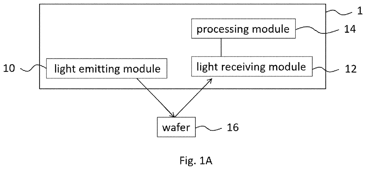
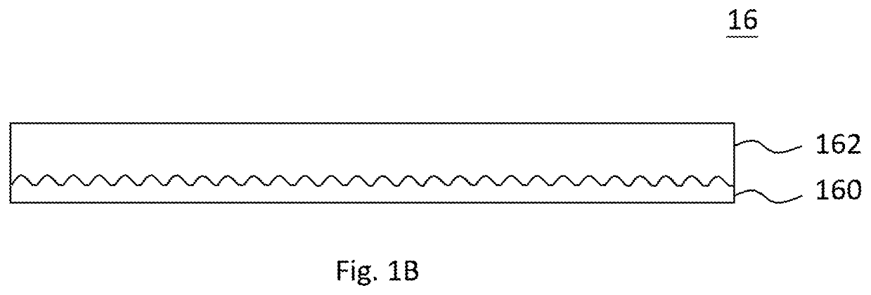
[0021]Please refer to FIG. 1A and Fig together. 1B, FIG. 1A is a block diagram of a wafer testing system in accordance with an embodiment of the present invention, and FIG. 1B is a schematic diagram of a wafer in accordance with an embodiment of the present invention. As shown in the figures, the wafer testing system 1 disclosed in this embodiment can be used to test the quality of the wafer 16. The wafer testing system 1 can comprises a light emitting module 10, a...


PUM


Abstract

Herein disclosed are a wafer, a wafer testing system, and a method thereof. Said wafer testing method comprises the following steps. First, an incident light is provided toward a wafer. And, a wafer surface image corresponded to the wafer is generated. Then, determining whether the wafer surface image has a plurality of first strips and a plurality of second strips, and the plurality of first strips and the plurality of second strips are symmetrical. When the wafer surface image has the plurality of first strips and the plurality of second strips, and the plurality of first strips and the plurality of second strips are symmetrical, a qualified signal corresponded to the wafer is provided

Description

CROSS REFERENCE TO RELATED APPLICATION[0001]The present application claims priority to Taiwan patent application Serial No. 108141700 filed on Nov. 18, 2019, the entire content of which is incorporated by reference to this application.BACKGROUND OF THE INVENTION1. Field of the Invention[0002]The present invention pertains to a semiconductor structure, a testing method and a testing system, in particular to a wafer, a non-contact wafer testing method and a wafer testing system2. Description of the Prior Art[0003]In general, in the manufacturing process of micro LEDs (μLEDs), various tests and inspections are required to determine the quality of the micro LED. For example, the testing procedure after an epitaxy process may include using a probe to contact electrodes of the micro LED, and then providing current through the probe to test whether the micro LED can emit light normally. However, due to the amount of micro LED in the wafer is huge, either to test the micro LEDs in the wafer...

Claims


Application Information

Patent Timeline
Patent Type & Authority Applications(United States)
IPC IPC(8): G01R31/302H01L33/00
CPCG01R31/302H01L33/005H01L33/0095G01R31/2656G01R31/2831
Inventor WU, JYUN-DELAI, YEN-LINCHEN, CHI-HENG
Owner PLAYNITRIDE DISPLAY CO LTD
Why Eureka
Try Eureka