

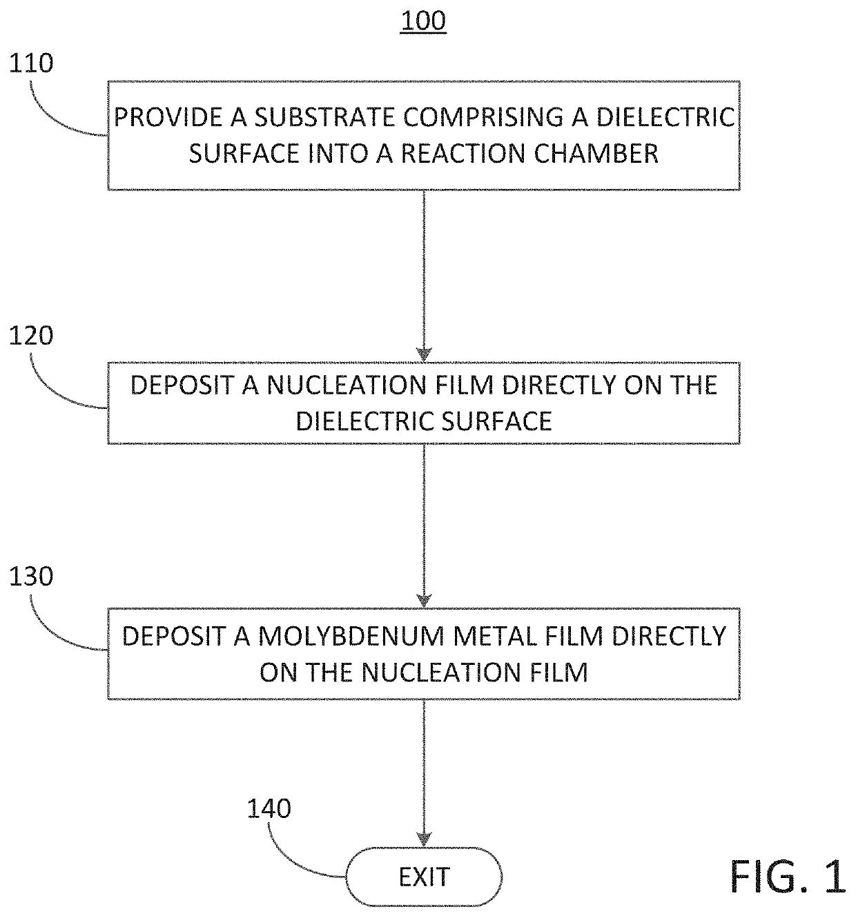
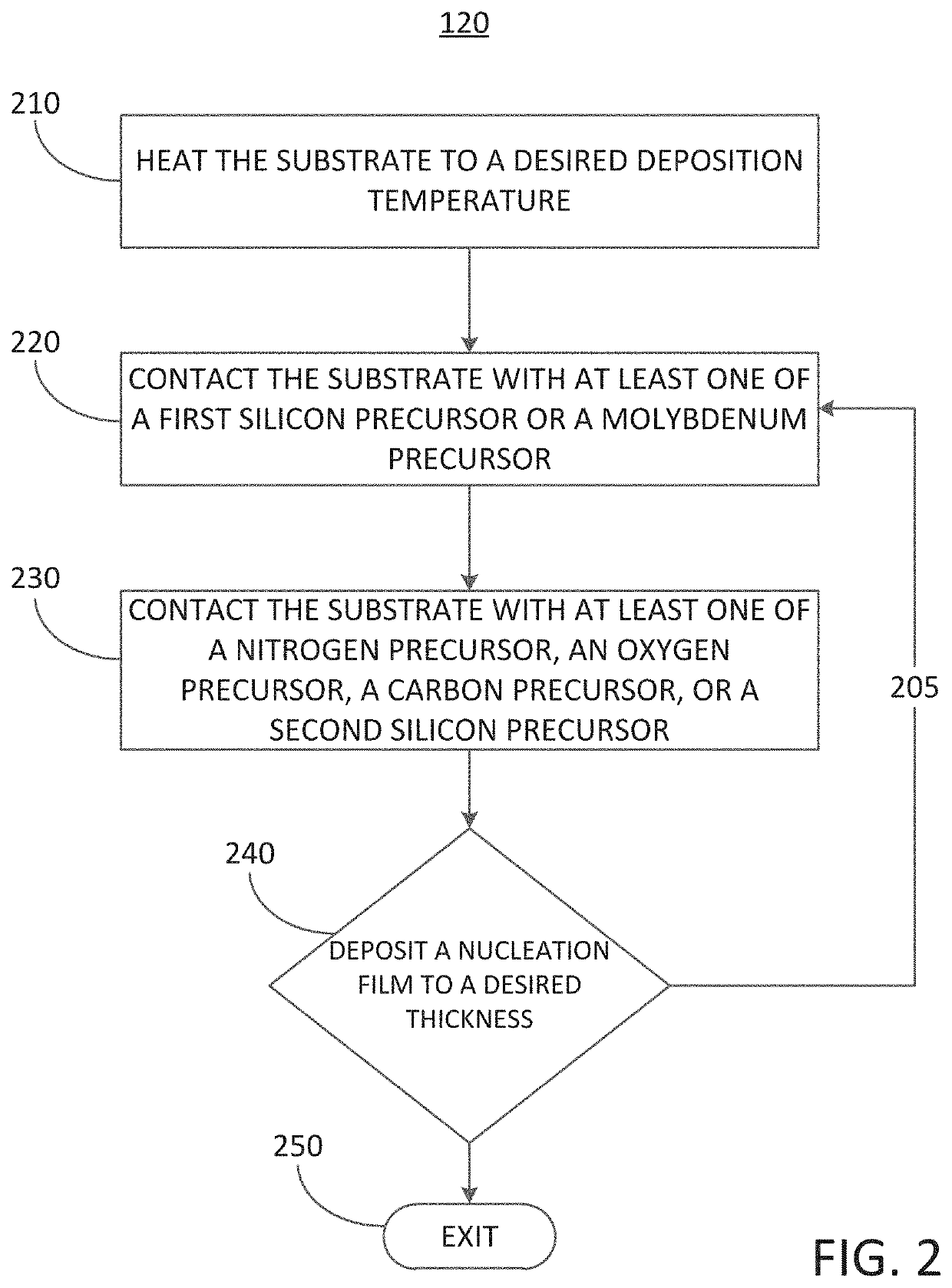
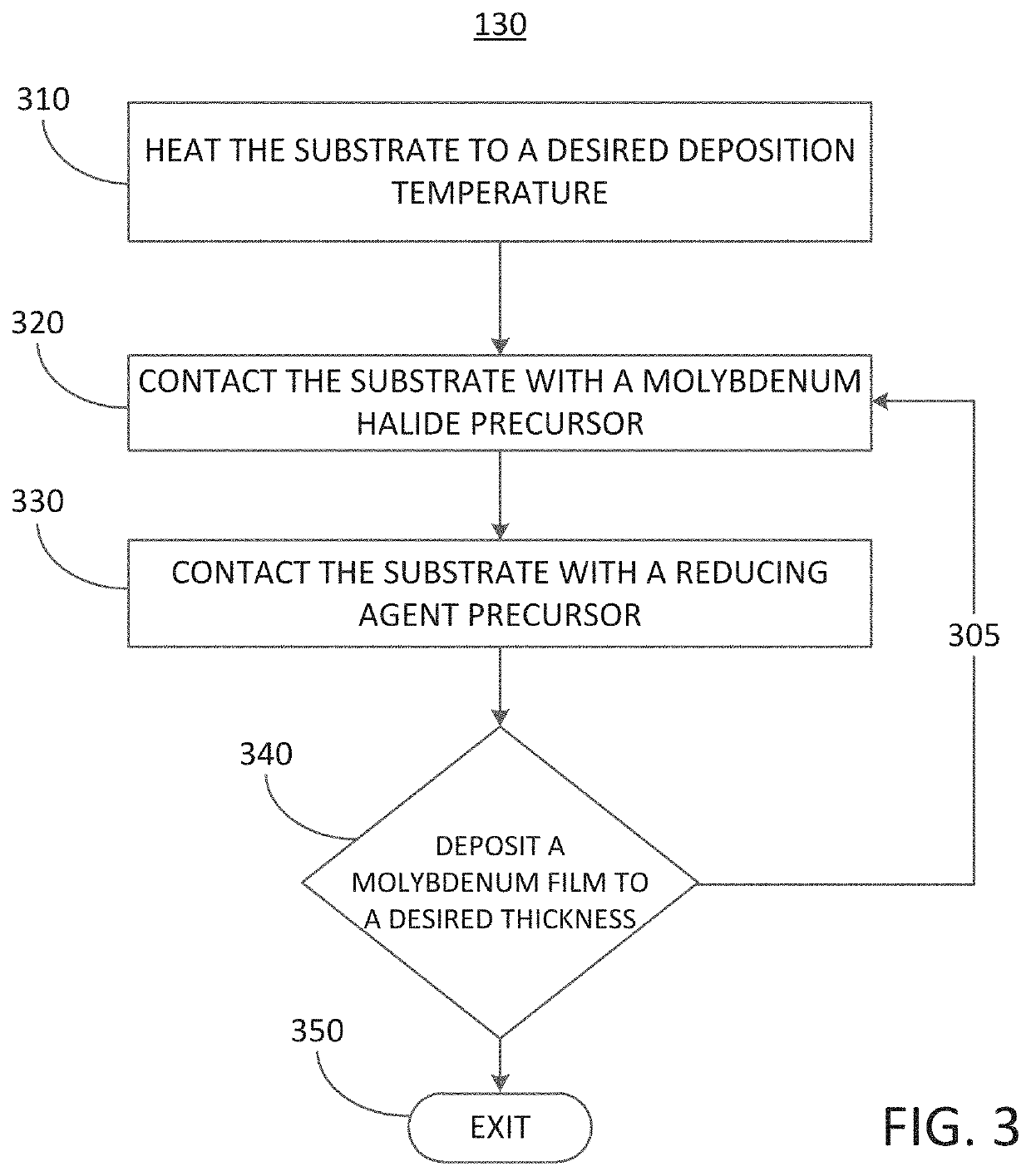
Methods for depositing a molybdenum metal film over a dielectric surface of a substrate by a cyclical deposition process and related semiconductor device structures
a molybdenum metal film and substrate technology, applied in the direction of semiconductor/solid-state device details, coatings, chemical vapor deposition coatings, etc., can solve the problem of increasing the overall electrical resistivity of the semiconductor device structur
- Summary
- Abstract
- Description
- Claims
- Application Information
AI Technical Summary
Benefits of technology
Problems solved by technology
Method used
Image

Examples
Embodiment Construction
[0020]Although certain embodiments and examples are disclosed below, it will be understood by those in the art that the invention extends beyond the specifically disclosed embodiments and / or uses of the invention and obvious modifications and equivalents thereof. Thus, it is intended that the scope of the invention disclosed should not be limited by the particular disclosed embodiments described below.
[0021]The illustrations presented herein are not meant to be actual views of any particular material, structure, or device, but are merely idealized representations that are used to describe embodiments of the disclosure.
[0022]As used herein, the term “substrate” may refer to any underlying material or materials that may be used, or upon which, a device, a circuit, or a film may be formed.
[0023]As used herein, the term “cyclic deposition” may refer to the sequential introduction of one or more precursors (reactants) into a reaction chamber to deposit a film over a substrate and include...
PUM
| Property | Measurement | Unit |
|---|---|---|
| thickness | aaaaa | aaaaa |
| aspect ratio | aaaaa | aaaaa |
| aspect ratio | aaaaa | aaaaa |
Abstract
Description
Claims
Application Information