Edge uniformity tunability on bipolar electrostatic chuck

a bipolar electrostatic chuck and uniform tunability technology, applied in the field of methods and systems with an electrostatic chuck, can solve the problems of reducing the effect of electrostatic charge in the wafer on the plasma, and achieve the effects of improving the tunability of ion flux, reducing the effect of electrostatic charge in the wafer, and improving the uniformity of deposited films

Pending Publication Date: 2021-05-27
APPLIED MATERIALS INC
View PDF10 Cites 2 Cited by
  • Summary
  • Abstract
  • Description
  • Claims
  • Application Information

AI Technical Summary

Benefits of technology

[0005]Embodiments of the present technology may allow for advantages in handling and processing substrates by using at least two bipolar electrodes and one annular electrode in the substrate support. The electrode configuration may allow for better tunability of ion flux near the edge of the wafer, which may result in higher uniformity of deposited films. In addition, the combination of bipolar electrodes and an annular electrode may reduce voltage needed to electrostatically chuck a wafer. The reduced voltage may result in less arcing and fewer wafer defects. Furthermore, embodiments of the present technology may reduce the effect of electrostatic charge in the wafer on the plasma. As a result, the plasma may be ignited after a wafer has been chucked rather than at the same time, and short-term plasma instabilities may be reduced during the ignition of the plasma.

Problems solved by technology

Furthermore, embodiments of the present technology may reduce the effect of electrostatic charge in the wafer on the plasma.

Method used


Image

  • Edge uniformity tunability on bipolar electrostatic chuck
  • Edge uniformity tunability on bipolar electrostatic chuck
  • Edge uniformity tunability on bipolar electrostatic chuck

Examples


Embodiment Construction

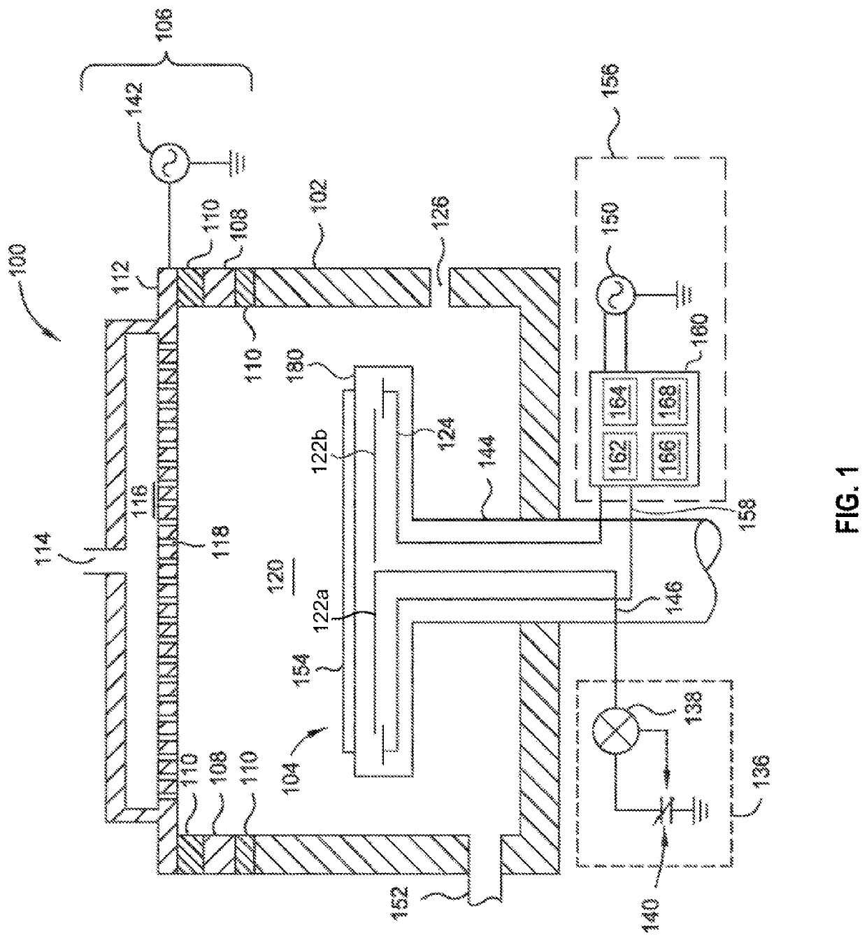
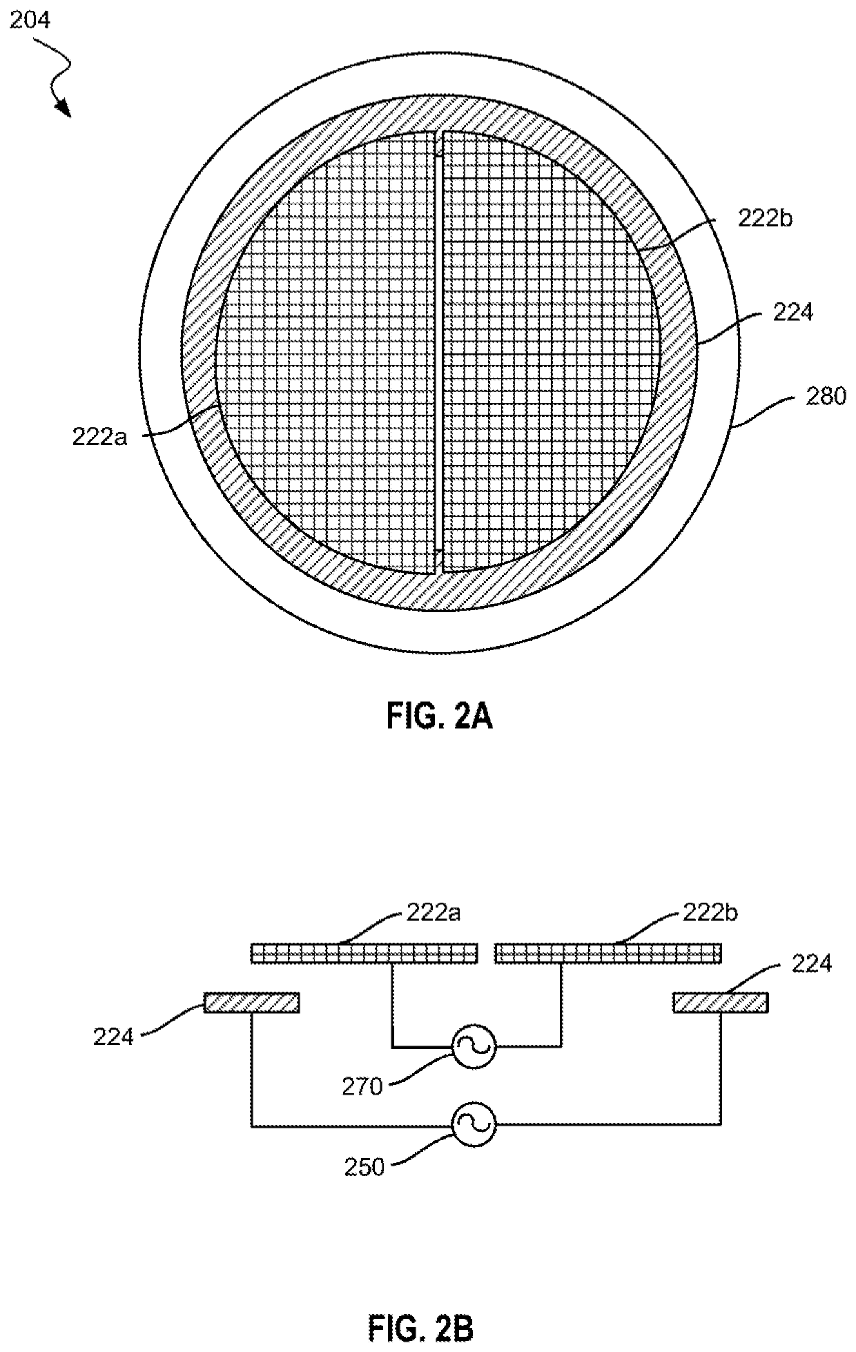
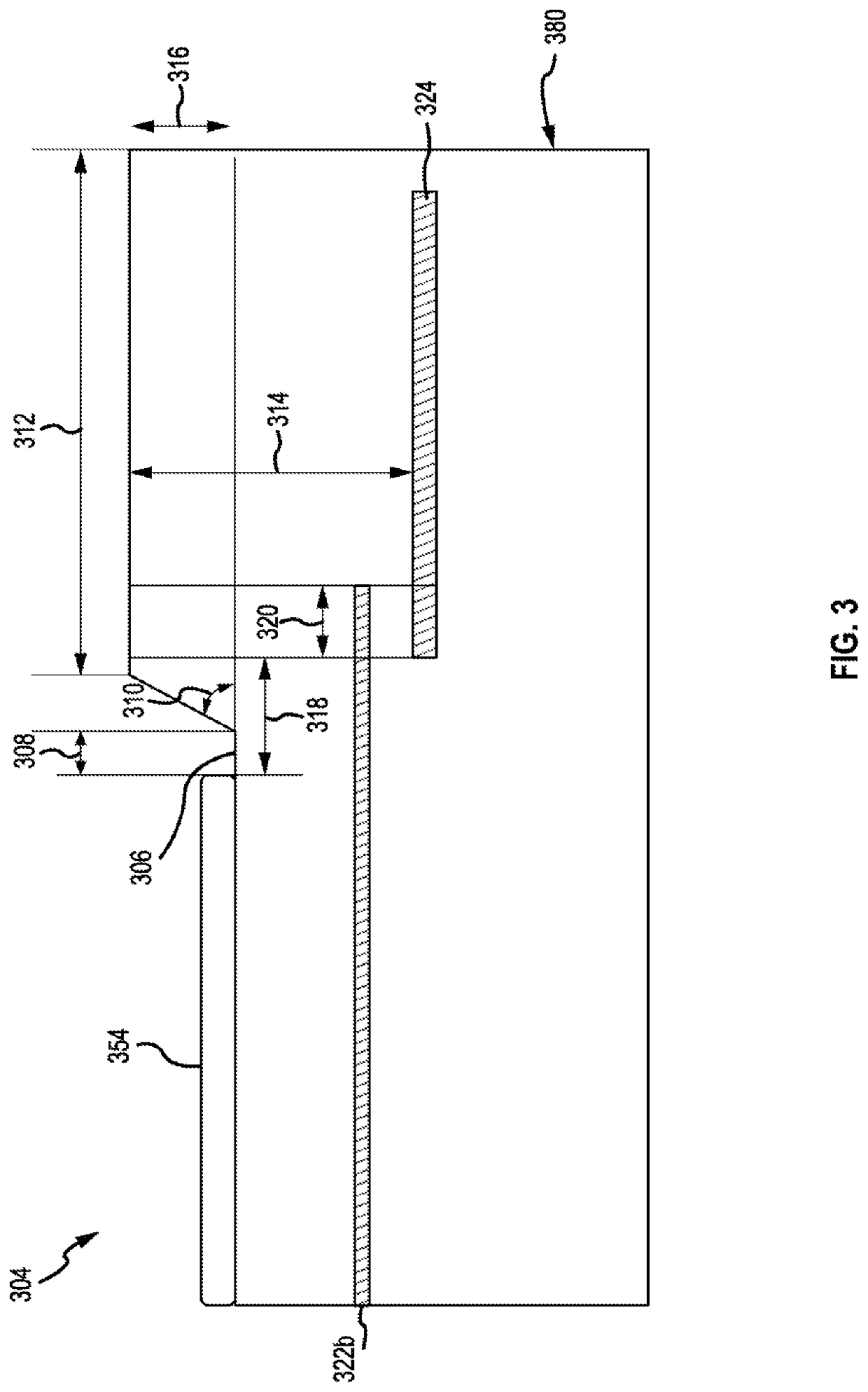
[0018]As characteristic dimensions of semiconductor devices decrease, processing becomes more complicated and additional challenges result. Layers deposited near the edge of a substrate may not be as uniform as those near the center of the substrate. The non-uniformities near the edge of the wafer may result in non-functional or poor performing devices, reducing yield and / or reliability. Wafers are often not completely flat and are electrostatically chucked to reduce any wafer bow. However, electrostatically chucking the wafer may result in arcing at the backside of the wafer. Previously when semiconductor devices were larger, arcing at the backside of the wafer may not have been a high concern, but processing to produce smaller devices sometimes includes materials deposited on the backside of the wafer. Such arcing may create defects on the backside of the wafer, which may in turn lead to defects on the frontside of the wafer. In addition, conventionally electrostatically chucking ...


PUM

PropertyMeasurementUnit
temperatureaaaaaaaaaa
voltageaaaaaaaaaa
resistanceaaaaaaaaaa

Abstract

Embodiments of the present technology may include an electrostatic chuck. The chuck may include a top surface, defining a recessed portion of the chuck. The recessed portion of the chuck may be configured to support a substrate. The chuck may further include a first electrode and a second electrode. The first electrode and the second electrode may be disposed within the chuck. The first electrode and the second electrode may be substantially coplanar. In addition, the chuck may include a third electrode. The third electrode may be disposed within the chuck. Furthermore, the third electrode may have an annular shape. The third electrode may be separated from the first electrode and the second electrode. In addition, the third electrode may be substantially parallel to the first electrode and the second electrode. Systems and methods including the electrostatic chuck are also described.

Description

FIELD[0001]The present technology relates to semiconductor substrate systems and methods. More specifically, the present technology relates to methods and systems with an electrostatic chuck having multiple electrodes.BACKGROUND[0002]In the manufacture of integrated circuits and other electronic devices, plasma processes are often used for deposition or etching of various material layers. For example, plasma-enhanced chemical vapor deposition (PECVD) process is a chemical process wherein electro-magnetic energy is applied to at least one precursor gas or precursor vapor to transform the precursor into a reactive plasma. Plasma may be generated inside the processing chamber, e.g., in-situ, or in a remote plasma generator that is remotely positioned from the processing chamber. This process is widely used to deposit materials on substrates to produce high-quality and high-performance semiconductor devices.[0003]In the current semiconductor manufacturing industry, transistor structures...

Claims


Application Information

Patent Timeline
Patent Type & Authority Applications(United States)
IPC IPC(8): H01L21/683H01J37/32C23C16/503C23C16/505C23C16/458
CPCH01L21/6833H01J37/32724H01J37/32541H01J37/32082H01J2237/3323C23C16/505C23C16/4586H01J2237/3321C23C16/503C23C16/4585C23C16/509C23C16/5096H01L21/68735
Inventor WOO, HYUNG JE
Owner APPLIED MATERIALS INC
Why Eureka
Try Eureka