
Manufacturing process for an optoelectronic device

Pending Publication Date: 2021-06-24
MERCK PATENT GMBH
View PDF3 Cites 0 Cited by
  • Summary
  • Abstract
  • Description
  • Claims
  • Application Information

AI Technical Summary

Benefits of technology

The present invention provides a new manufacturing process for optoelectronic devices that allows for the well-defined and controlled deposition of uniform coatings of wavelength converting material on optoelectronic device precursors. This process offers an opportunity to specifically adjust the color distribution, color temperature, and color point of the device with sufficient stability. Additionally, the invention provides a new manufacturing process that is suitable for large-scale mass production and allows for faster curing at lower temperatures to avoid thermal stress on the optoelectronic device package.

Problems solved by technology

When generating white light with such an arrangement, it is difficult to generate white light of a desired colour point due to variations in the colour point, luminance, and other factors of the wavelength converting materials.
Unevenness in colour may also be caused by failure to uniformly mix the light emitted by the wavelength converting materials or to uniformly coat the light emitting diodes with the wavelength converting materials.
Typical curing conditions for silicones are 4 h at 150° C. However, silicone-based materials suffer from various disadvantages such as a high gas permeability, outgassing of volatile organic compounds, a low refractive index and yellow discolouration which may lead to a reduced lifetime, reduced efficiency and undesired deviation of colour point.
However, the curing of polysilazanes is much slower than the curing of silicones and needs higher temperatures which is a major challenge in terms of compatibility with the LED precursor.
Not all LED precursors tolerate such high temperatures without suffering from damage.

Method used


Image

  • Manufacturing process for an optoelectronic device
  • Manufacturing process for an optoelectronic device
  • Manufacturing process for an optoelectronic device

Examples


example 1

[0156]A dispersion of 10 g of the organopolysiloxazane Material A, 15 g phosphor (YGA 200 547) and 50 ml ethyl acetate was sprayed on an Excelitas LED package (LED precursor) in three layers of each ca. 10 μm thickness in average. After spraying of each layer the LED package was exposed to an IR emitter described in FIG. 8 for 1 min. After the 1 min exposure the coating was dry-to-touch and the colour coordinates were measured. Then the process was repeated: spraying three layers, curing each layer by IR exposure and finally measuring the colour coordinates. The data obtained from both colour-point measurements were used to calculate the number of the remaining layers necessary to reach the target colour point of x / y=0.400 / 0.377. After spraying the required number of the calculated remaining layers (usually 2, 3 or 4) and curing each layer by IR exposure, the LED package was finally cured on a hotplate at 220° C. for 4 h. This process was used to prepare a number of 25 LEDs to have ...

example 2

ng

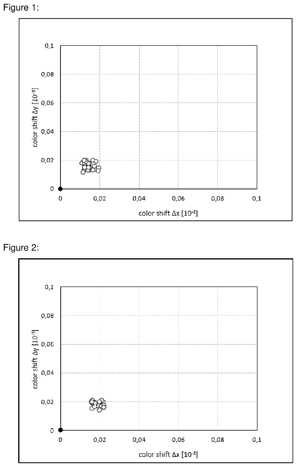
[0158]25 LEDs were prepared according to the procedure described in Example 1, except that the IR exposure was replaced by UV-C exposure for 1 min with a UV-lamp as described in FIG. 9. The results are shown in Table 1.

[0159]FIG. 2 shows the colour coordinate shift resulting after final curing, wherein the colour coordinates before final curing are set to zero.

example 3 (

Reference Example): Thermal Curing

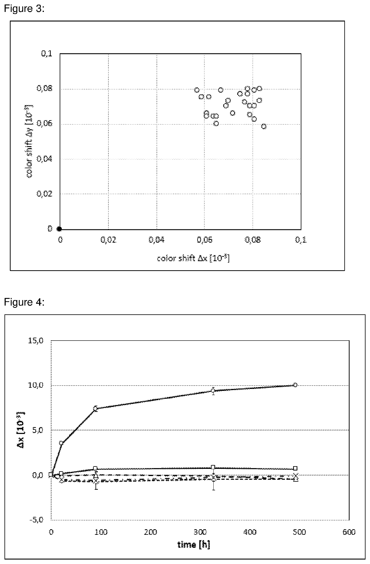
[0160]25 LEDs were prepared according to the procedure described in Example 1, except that the IR exposure was replaced by thermal curing on a hotplate at 150° C. for 1 min. After the thermal curing the coating was still sticky. The results are shown in Table 1. FIG. 3 shows the colour coordinate shift resulting after final curing, wherein the colour coordinates before final curing are set to zero.

TABLE 1Standard deviation a of the colour coordinates x and y andaverage colour point shift of x- and y-coordinate after full curing, calculated for 25 devices.averageaveragecolour colour σσpoint shift point shift Examplex-coordinatey-coordinatex-coordinatey-coordinateExample 1 0.00250.00280.0160.015(IR)Example 2 0.00230.00230.0190.018(UV-C)Example 30.00720.00630.0710.071(reference,thermal curing)

[0161]The standard deviation a of the colour coordinates x and y of the IR- and UV-precured LEDs is much smaller when compared to the thermally cured reference LE...


PUM

PropertyMeasurementUnit
Thicknessaaaaaaaaaa
Wavelengthaaaaaaaaaa

Abstract

The present invention relates to a process for manufacturing an optoelectronic device, wherein a layer of a formulation containing a silazane polymer and a wavelength converting material is applied to an optoelectronic device precursor, precured by exposure to radiation and then cured. There is further provided an optoelectronic device, preferably a light emitting device (LED) or a micro-light emitting device (micro-LED), which is prepared by said manufacturing process.

Description

TECHNICAL FIELD OF THE INVENTION[0001]The present invention relates to a process for manufacturing an optoelectronic device, wherein a layer of a formulation containing a silazane polymer and a wavelength converting material is applied to an optoelectronic device precursor and precured by exposure to radiation. This process is successively carried out two or more times so that an optoelectronic device precursor comprising two or more precured layers arranged one above the other is obtained. The precured layers on the optoelectronic device precursor are then cured by exposure to heat or radiation. The present invention further relates to an optoelectronic device, preferably a light emitting device (LED) or a micro-light emitting device (micro-LED), which is prepared by said manufacturing process. The manufacturing process of the present invention allows a cost-efficient and fast production of optoelectronic devices, where the respectively desired colour point of the wavelength conver...

Claims


Application Information

Patent Timeline
IPC IPC(8): H01L33/50C09K11/02C08G77/62C08G77/54
CPCH01L33/502C09K11/02H01L2933/0041C08G77/54C08G77/62H01L33/501H01L33/504H01L33/52H01L33/56H01L2933/005
Inventor GROTTENMUELLER, RALFCASAS GARCIA-MINGUILLAN, ABRAHAMKITA, FUMIOLANDMANN, CHRISTOPHBLUMENSCHEIN, FABIAN
Owner MERCK PATENT GMBH
Learn More