Opto-electronic device having junction field-effect transistor structure and method of manufacturing the same

a transistor and junction field technology, applied in the direction of electrical equipment, semiconductor devices, radio control devices, etc., can solve the problems of difficult to obtain clear images, low signal-to-noise ratio, etc., and achieve low dark noise and high signal-to-noise ratio

Active Publication Date: 2021-08-12
SAMSUNG ELECTRONICS CO LTD
View PDF5 Cites 0 Cited by
  • Summary
  • Abstract
  • Description
  • Claims
  • Application Information

AI Technical Summary

Benefits of technology

[0004]Provided are opto-electronic devices with low dark noise and high signal-to-noise ratio.

Problems solved by technology

Accordingly, a fraction of dark noise in a signal output from the light receiving element of the pixel is relatively increased and a signal-to-noise ratio is lowered, and thus, it difficult to obtain a clear image.

Method used


Image

  • Opto-electronic device having junction field-effect transistor structure and method of manufacturing the same
  • Opto-electronic device having junction field-effect transistor structure and method of manufacturing the same
  • Opto-electronic device having junction field-effect transistor structure and method of manufacturing the same

Examples


Embodiment Construction

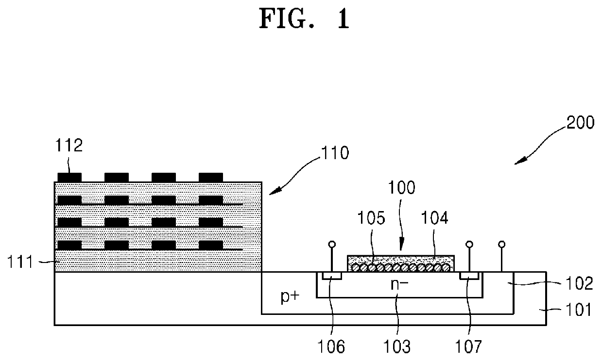
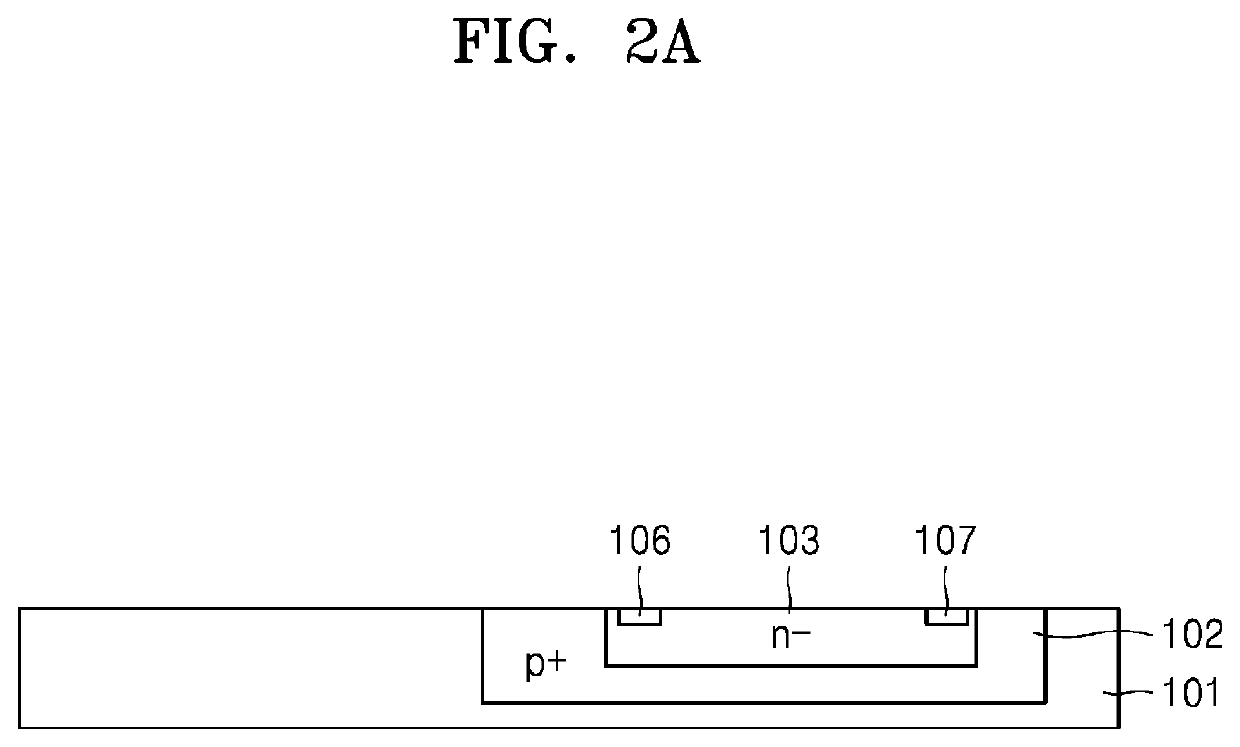
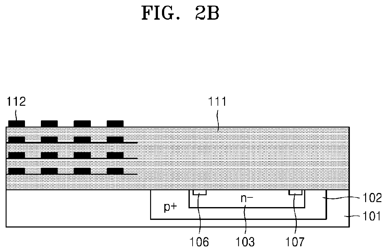
[0037]Reference will now be made in detail to embodiments, examples of which are illustrated in the accompanying drawings, wherein like reference numerals refer to like elements throughout. In this regard, the embodiments may have different forms and should not be construed as being limited to the descriptions set forth herein. Accordingly, the embodiments are merely described below, by referring to the figures, to explain aspects. As used herein, the term “and / or” includes any and all combinations of one or more of the associated listed items. Expressions such as “at least one of,” when preceding a list of elements, modify the entire list of elements and do not modify the individual elements of the list.

[0038]Hereinafter, opto-electronic devices having a junction field-effect transistor structure and methods of manufacturing the same will be described in detail with reference to the accompanying drawings. In the drawings, like reference numerals refer to like elements, and sizes of...


PUM

PropertyMeasurementUnit
pixel sizeaaaaaaaaaa
diameteraaaaaaaaaa
thicknessaaaaaaaaaa

Abstract

Provided are opto-electronic devices with low dark noise and high signal-to-noise ratio and methods of manufacturing the same. An opto-electronic device may include: a semiconductor substrate; a light receiving unit formed in the semiconductor substrate; and a driving circuit arranged on a surface of the semiconductor substrate. The light receiving unit may include: a first semiconductor layer partially arranged in an upper region of the semiconductor substrate and doped with a first conductivity type impurity; a second semiconductor layer arranged on the first semiconductor layer and doped with a second conductivity type impurity; a transparent matrix layer arranged on an upper surface of the second semiconductor layer; a plurality of quantum dots arranged to contact the transparent matrix layer; and a first electrode and a second electrode electrically connected to the second semiconductor layer and respectively arranged on both sides of the transparent matrix layer.

Description

CROSS-REFERENCE TO RELATED APPLICATION[0001]This application is based on and claims priority from Korean Patent Application No. 10-2020-0014354, filed on Feb. 6, 2020, in the Korean Intellectual Property Office, the disclosure of which is incorporated herein in its entirety by reference.BACKGROUND1. Field[0002]The disclosure relates to opto-electronic devices having a junction field-effect transistor structure and methods of fabricating the same, and more particularly, to quantum dot opto-electronic devices having a junction field-effect transistor structure and methods of fabricating the same.2. Description of Related Art[0003]Recently, image sensors with high resolution are widely used in electronic devices. As the resolution of an image sensor increases, the size of one pixel in the image sensor gradually decreases. For example, the pixel size of a high resolution image sensor used in mobile phones has become less than 1 μm. When the size of a pixel is reduced as described above,...

Claims


Application Information

Patent Timeline
Patent Type & Authority Applications(United States)
IPC IPC(8): H01L27/146
CPCH01L27/1461H01L27/14683H01L27/14612H01L27/14679H01L27/1462H01L31/035218H01L31/1129
Inventor CHO, KYUNGSANGKIM, HOJUNGBAIK, CHANWOOK
Owner SAMSUNG ELECTRONICS CO LTD
Why Eureka
Try Eureka